ZHCSGB3A June 2017 – August 2018 ESD122
PRODUCTION DATA.
- 1 特性
- 2 应用
- 3 说明
- 4 修订历史记录
- 5 Pin Configuration and Functions
- 6 Specifications
-
7 Detailed Description
- 7.1 Overview
- 7.2 Functional Block Diagram
- 7.3
Feature Description
- 7.3.1 IEC 61000-4-2 ESD Protection
- 7.3.2 IEC 61000-4-4 EFT Protection
- 7.3.3 IEC 61000-4-5 Surge Protection
- 7.3.4 IO Capacitance
- 7.3.5 DC Breakdown Voltage
- 7.3.6 Ultra Low Leakage Current
- 7.3.7 Low ESD Clamping Voltage
- 7.3.8 Supports High Speed Interfaces
- 7.3.9 Industrial Temperature Range
- 7.3.10 Easy Flow-Through Routing Package
- 7.4 Device Functional Modes
- 8 Application and Implementation
- 9 Power Supply Recommendations
- 10Layout
- 11器件和文档支持
- 12机械、封装和可订购信息
7.4 Device Functional Modes
The ESD122 is a passive circuit that triggers when voltages are above VBRF or below VBRR. During ESD events, voltages as high as ±17 kV (contact) can be directed to ground via the internal diode network. When the voltages on the protected line fall below the trigger levels of ESD122 (usually within 10s of nano-seconds) the device reverts to passive.
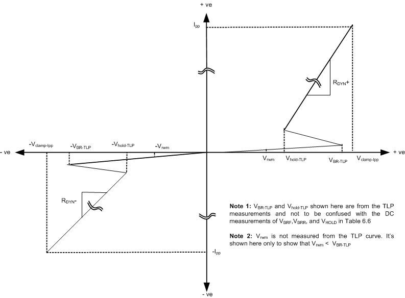
Figure 12 shows typical TLP behavior of bi-directional ESD device.
 Figure 12. Generic TLP I-V Curve for a Bi-Directional ESD Device
for the Illustration of Vrwm, VBR, Vhold and Vclamp