SNLS302E May 2010 – February 2015 DS92LV2411 , DS92LV2412
PRODUCTION DATA.
- 1 Features
- 2 Applications
- 3 Description
- 4 Revision History
- 5 Pin Configuration and Functions
-
6 Specifications
- 6.1 Absolute Maximum Ratings
- 6.2 ESD Ratings
- 6.3 Recommended Operating Conditions
- 6.4 Thermal Information
- 6.5 Serializer DC Electrical Characteristics
- 6.6 Deserializer DC Electrical Characteristics
- 6.7 DC and AC Serial Control Bus Characteristics
- 6.8 Recommended Timing For The Serial Control Bus
- 6.9 Recommended Serializer Timing For CLKIN
- 6.10 Serializer Switching Characteristics
- 6.11 Deserializer Switching Characteristics
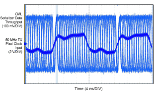
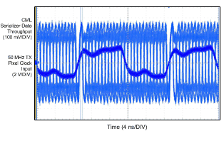
- 6.12 Typical Characteristics
-
7 Detailed Description
- 7.1 Overview
- 7.2 Functional Block Diagrams
- 7.3
Feature Description
- 7.3.1 Serializer Functional Description
- 7.3.2
Deserializer Functional Description
- 7.3.2.1 Integrated Signal Conditioning Features — Des
- 7.3.2.2 EMI Reduction Features
- 7.3.2.3 Power Saving Features
- 7.3.2.4 Des — Clock-Data Recovery Status Flag (Lock) And Output State Select (OSS_SEL)
- 7.3.2.5 Des — Oscillator Output — Optional
- 7.3.2.6 Des — OP_LOW — Optional
- 7.3.2.7 Des — Clock Edge Select (RFB)
- 7.3.2.8 Des — Control Signal Filter — Optional
- 7.3.2.9 Des — SSCG Low Frequency Optimization (Lf_mode)
- 7.3.2.10 Des — Strap Input Pins
- 7.3.3 Built In Self Test (BIST)
- 7.4 Device Functional Modes
- 7.5 Programming
- 7.6 Register Maps
- 8 Applications and Implementation
- 9 Power Supply Recommendations
- 10Layout
- 11Device and Documentation Support
- 12Mechanical, Packaging, and Orderable Information
8 Applications and Implementation
8.1 Application Information
The DS92LV2411/DS92LV2412 chipset is intended for interface between a host (graphics processor) and a Display. It supports an 24-bit color depth (RGB888). In a RGB888 application, 24 color bits (D[23:0), Pixel Clock (CLKIN) and three control bits (C1, C2, C3) are supported across the serial link with CLK rates from 5 to 50 MHz. The chipset may also be used in 18-bit color applications. In this application three to six general purpose signals may also be sent from host to display.
The Des is expected to be located close to its target device. The interconnect between the Des and the target device is typically in the 1 to 3 inch separation range. The input capacitance of the target device is expected to be in the 5 to 10 pF range. Care should be taken on the CLK output trace as this signal is edge sensitive and strobes the data. It is also assumed that the fanout of the Des is one. If additional loads need to be driven, a logic buffer or mux device is recommended.
8.2 Typical Applications
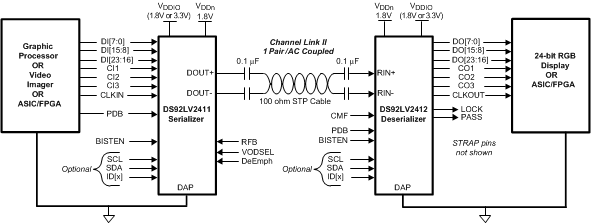 Figure 34. Typical Application Schematic for DS92LV2411, DS92LV2412 Ser/Des Pair
8.2.1 Design Requirements
For this typical design application, use the following as input parameters.
Table 15. Design Parameters
| DESIGN PARAMETER | EXAMPLE VALUE |
|---|---|
| VDDIO | 1.8 V or 3.3 V |
| VDDn | 1.8 V |
| AC Coupling Capacitor for DOUT± and RIN± | 0.1 µF |
| CLK Frequency | 50 MHz |
8.2.2 Detailed Design Procedure
8.2.2.1 Typical Application Connection
Figure 35 shows a typical connection diagram of the DS92LV2411 Ser in Pin control mode for a 24-bit application. The CML outputs require 0.1 µF AC coupling capacitors to the line. The line driver includes internal termination. Bypass capacitors are placed near the power supply Pins. At a minimum, four 0.1 µF capacitors and a 4.7 µF capacitor should be used for local device bypassing. System GPO (General Purpose Output) signals control the PDB and BISTEN Pins. In this application the RFB Pin is tied Low to latch data on the falling edge of the CLKIN. In this example the cable is long, therefore the VODSEL Pin is tied High and a De-Emphasis value is selected by the resistor R1. The interface to the host is with 1.8 V LVCMOS levels, thus the VDDIO Pin is connected also to the 1.8V rail. The optional Serial Bus control is not used in this example, thus the SCL, SDA and ID[x] Pins are left open. A delay cap is placed on the PDB signal to delay the enabling of the device until power is stable.
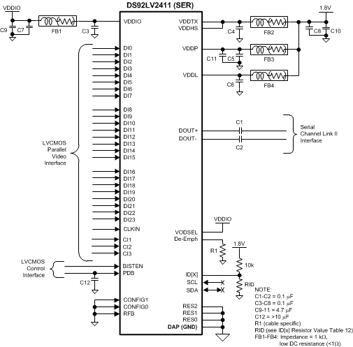 Figure 35. DS92LV2411 Typical Connection Diagram — Pin Control
Figure 36 shows a typical connection diagram of the DS92LV2412 Des in Pin/strap control mode for a 24-bit application. The CML inputs utilize 0.1 µF coupling capacitors to the line and the receiver provides internal termination. Bypass capacitors are placed near the power supply Pins. At a minimum, seven 0.1 µF capacitors and two 4.7 µF capacitors should be used for local device bypassing. System GPO (General Purpose Output) signals control the PDB and the BISTEN Pins. In this application the RFB Pin is tied Low to strobe the data on the falling edge of the CLKOUT.
Since the device in the Pin/STRAP mode, four 10 kΩ pull up resistors are used on the parallel output bus to select the desired device features. CFEN is set to 1 for Normal Mode with Control Signal Filter enabled, this is accomplished with the STRAP pull-up on DO23. The receiver input equalizer is also enabled and set to provide 7.5 dB of gain, this is accomplished with EQ[3:0] set to 1001'b with STRAP pull ups on DO12 and DO15. To reduce parallel bus EMI, the SSCG feature is enabled and set to fmod = CLK/2168 and ±1% with SSC[3:0] set to 0010'b and a STRAP pull-up on DO4. The desired features are set with the use of the four pull up resistors.
The interface to the target display is with 3.3V LVCMOS levels, thus the VDDIO Pin is connected to the 3.3 V rail. The optional Serial Bus Control is not used in this example, thus the SCL, SDA and ID[x] Pins are left open. A delay cap is placed on the PDB signal to delay the enabling of the device until power is stable.
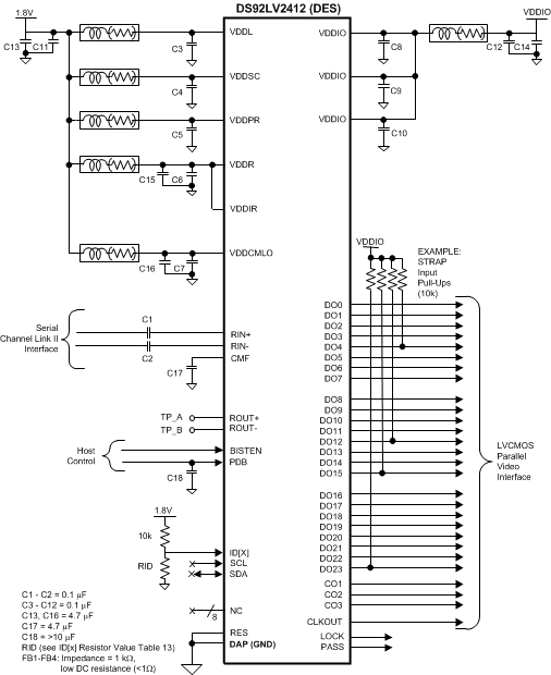 Figure 36. DS92LV2412 Typical Connection Diagram — Pin Control
8.2.2.2 Power Up Requirements and PDB Pin
The VDD (VDDn and VDDIO) supply ramp should be faster than 1.5 ms with a monotonic rise. If slower then 1.5 ms then a capacitor on the PDB Pin is needed to ensure PDB arrives after all the VDD have settled to the recommended operating voltage. When PDB Pin is pulled to VDDIO, it is recommended to use a 10 kΩ pull-up and a 22 uF cap to GND to delay the PDB input signal.
8.2.2.3 Transmission Media
The Ser/Des chip set is intended to be used in a point-to-point configuration, through a PCB trace, through twisted pair cable or through 50Ω coaxial cables. The Ser and Des provide internal terminations providing a clean signaling environment. The interconnect for the differential serial interface should present a differential impedance of 100Ω. Use cables and connectors that have matched differential impedance to minimize impedance discontinuities. Shielded or un-shielded cables may be used depending upon the noise environment and application requirements.
For 50Ω coaxial cable serial interfaces, any unused input or output Pin must be terminated with an 0.1 µF AC coupling capacitor and a 50Ω resistor to ground. The PCB traces and serial interconnect should have a single ended impedance of 50Ω.
8.2.2.4 Live Link Insertion
The Ser and Des devices support live pluggable applications. The automatic receiver lock to random data “plug and go” hot insertion capability allows the DS92LV2412 to attain lock to the active data stream during a live insertion event.
8.2.2.5 Serial Interconnect Guidelines
See AN-1108 (SNLA008) and AN-905 (SNLA035) for full details.
- Use 100Ω coupled differential pairs
- Use the S/2S/3S rule in spacings
- S = space between the pair
- 2S = space between pairs
- 3S = space to LVCMOS signal
- Minimize the number of Vias
- Use differential connectors when operating above 500Mbps line speed
- Maintain balance of the traces
- Minimize skew within the pair
- Terminate as close to the TX outputs and RX inputs as possible
Additional general guidance can be found in the LVDS Owner’s Manual - available in PDF format from the Texas Instruments web site at: http://www.ti.com/ww/en/analog/interface/lvds.shtml