SNLS045C July 1999 – July 2016 DS90LV048A
PRODUCTION DATA.
- 1 Features
- 2 Applications
- 3 Description
- 4 Revision History
- 5 Pin Configuration and Functions
- 6 Specifications
- 7 Parameter Measurement Information
- 8 Detailed Description
- 9 Application and Implementation
- 10Power Supply Recommendations
- 11Layout
- 12Device and Documentation Support
- 13Mechanical, Packaging, and Orderable Information
6 Specifications
6.1 Absolute Maximum Ratings
See (1)(2)| MIN | MAX | UNIT | |||
|---|---|---|---|---|---|
| Supply voltage (VCC) | –0.3 | 4 | V | ||
| Input voltage (RIN+, RIN−) | –0.3 | 3.6 | V | ||
| Enable input voltage (EN, EN*) | –0.3 | VCC + 0.3 | V | ||
| Output voltage (ROUT) | –0.3 | VCC + 0.3 | V | ||
| Maximum package power dissipation at +25°C | D0016A package | 1025 | mW | ||
| PW0016A package | 866 | ||||
| Derate D0016A package | above +25°C | 8.2 | mW/°C | ||
| Derate PW0016A package | above +25°C | 6.9 | |||
| Lead temperature soldering | (4 s) | 260 | °C | ||
| Maximum junction temperature | 150 | °C | |||
| Storage temperature, Tstg | –65 | 150 | °C | ||
(1) Stresses beyond those listed under Absolute Maximum Ratings may cause permanent damage to the device. These are stress ratings only, which do not imply functional operation of the device at these or any other conditions beyond those indicated under Recommended Operating Conditions. Exposure to absolute-maximum-rated conditions for extended periods may affect device reliability.
(2) If Military/Aerospace specified devices are required, please contact the Texas Instruments Sales Office/Distributors for availability and specifications.
6.2 ESD Ratings
| VALUE | UNIT | |||
|---|---|---|---|---|
| V(ESD) | Electrostatic discharge(1) | Human-body model (HBM) | ±10000 | V |
| Machine model | ±1200 | |||
(1) ESD Rating:
HBM (1.5 kΩ, 100 pF)
EIAJ (0 Ω, 200 pF)
HBM (1.5 kΩ, 100 pF)
EIAJ (0 Ω, 200 pF)
6.3 Recommended Operating Conditions
| MIN | NOM | MAX | UNIT | |
|---|---|---|---|---|
| Supply voltage, VCC | 3 | 3.3 | 3.6 | V |
| Receiver input voltage | GND | 3 | V | |
| Operating free air temperature, TA | −40 | 25 | 85 | °C |
6.4 Thermal Information
| THERMAL METRIC(1) | DS90LV048A | UNIT | |
|---|---|---|---|
| PW (TSSOP) | |||
| 16 PINS | |||
| RθJA | Junction-to-ambient thermal resistance | 110.2 | °C/W |
| RθJC(top) | Junction-to-case (top) thermal resistance | 47 | °C/W |
| RθJB | Junction-to-board thermal resistance | 54.7 | °C/W |
| ψJT | Junction-to-top characterization parameter | 6.1 | °C/W |
| ψJB | Junction-to-board characterization parameter | 54.2 | °C/W |
(1) For more information about traditional and new thermal metrics, see the Semiconductor and IC Package Thermal Metrics application report.
6.5 Electrical Characteristics
Over Supply Voltage and Operating Temperature ranges, unless otherwise specified.(1)(2)| PARAMETER | TEST CONDITIONS | PIN | MIN | TYP | MAX | UNIT | ||
|---|---|---|---|---|---|---|---|---|
| VTH | Differential input high threshold | VCM = +1.2 V, 0.05 V, 2.95 V(3) | RIN+, RIN− | −35 | 0 | mV | ||
| VTL | Differential input low threshold | −100 | −35 | mV | ||||
| VCMR | Common-mode voltage range | VID = 200 mV peak to peak?(4) | 0.1 | 2.3 | V | |||
| IIN | Input current | VIN = +2.8 V | VCC = 3.6 V or 0 V | −10 | ±5 | 10 | μA | |
| VIN = 0 V | −10 | ±1 | 10 | |||||
| VIN = +3.6 V | VCC = 0 V | –20 | ±1 | 20 | ||||
| VOH | Output high voltage | IOH = −0.4 mA, VID = +200 mV | ROUT | 2.7 | 3.3 | V | ||
| IOH = −0.4 mA, input terminated | 2.7 | 3.3 | ||||||
| IOH = −0.4 mA, input shorted | 2.7 | 3.3 | ||||||
| VOL | Output low voltage | IOL = 2 mA, VID = −200 mV | 0.05 | 0.25 | V | |||
| IOS | Output short-circuit current | Enabled, VOUT = 0 V(5) | −15 | −47 | −100 | mA | ||
| IOZ | Output TRI-STATE current | Disabled, VOUT = 0 V or VCC | −10 | ±1 | 10 | μA | ||
| VIH | Input high voltage | EN, EN* | 2 | VCC | V | |||
| VIL | Input low voltage | GND | 0.8 | V | ||||
| II | Input current | VIN = 0 V or VCC, other Input = VCC or GND | −10 | ±5 | 10 | μA | ||
| VCL | Input clamp voltage | ICL = −18 mA | −1.5 | −0.8 | V | |||
| ICC | No load supply current receivers enabled |
EN = VCC, inputs open | VCC | 9 | 15 | mA | ||
| ICCZ | No load supply current receivers disabled |
EN = GND, inputs open | 1 | 5 | mA | |||
(1) Current into device pins is defined as positive. Current out of device pins is defined as negative. All voltages are referenced to ground unless otherwise specified.
(2) All typicals are given for: VCC = 3.3 V, TA = 25°C.
(3) VCC is always higher than RIN+ and RIN− voltage. RIN− and RIN+ are allowed to have a voltage range −0.2 V to VCC− VID/2. However, to be compliant with AC specifications, the common voltage range is 0.1 V to 2.3 V.
(4) The VCMR range is reduced for larger VID. Example: if VID = 400 mV, the VCMR is 0.2 V to 2.2 V. The fail-safe condition with inputs shorted is not supported over the common-mode range of 0 V to 2.4 V, but is supported only with inputs shorted and no external common-mode voltage applied. A VID up to VCC – 0 V may be applied to the RIN+/ RIN− inputs with the Common-Mode voltage set to VCC/2. Propagation delay and Differential Pulse skew decrease when VID is increased from 200 mV to 400 mV. Skew specifications apply for 200 mV ≤ VID ≤ 800 mV over the common-mode range.
(5) Output short-circuit current (IOS) is specified as magnitude only; minus sign indicates direction only. Only one output should be shorted at a time; do not exceed maximum junction temperature specification.
6.6 Switching Characteristics
Over Supply Voltage and Operating Temperature ranges, unless otherwise specified.(1)(2)(4)(5)| PARAMETER | TEST CONDITIONS | MIN | TYP | MAX | UNIT | |
|---|---|---|---|---|---|---|
| tPHLD | Differential propagation delay high to low | CL = 15 pF VID = 200 mV (Figure 15 and Figure 16) |
1.2 | 2 | 2.7 | ns |
| tPLHD | Differential propagation delay low to high | 1.2 | 1.9 | 2.7 | ns | |
| tSKD1 | Differential pulse skew |tPHLD − tPLHD|(3) | 0 | 0.1 | 0.4 | ns | |
| tSKD2 | Differential channel-to-channel skew; same device(4) | 0 | 0.15 | 0.5 | ns | |
| tSKD3 | Differential part-to-part skew(5) | 1 | ns | |||
| tSKD4 | Differential part-to-part skew(6) | 1.5 | ns | |||
| tTLH | Rise time | 0.5 | 1 | ns | ||
| tTHL | Fall time | 0.35 | 1 | ns | ||
| tPHZ | Disable time high to Z | RL = 2 kΩ CL = 15 pF (Figure 17 and Figure 18) |
8 | 14 | ns | |
| tPLZ | Disable time low to Z | 8 | 14 | ns | ||
| tPZH | Enable time Z to high | 9 | 14 | ns | ||
| tPZL | Enable time Z to low | 9 | 14 | ns | ||
| fMAX | Maximum operating frequency(7) | All channels switching | 200 | 250 | MHz | |
(1) All typicals are given for: VCC = 3.3 V, TA = 25°C.
(2) Generator waveform for all tests unless otherwise specified: f = 1 MHz, ZO = 50 Ω, tr and tf (0% to 100%) ≤ 3 ns for RIN.
(3) tSKD1 is the magnitude difference in differential propagation delay time between the positive going edge and the negative going edge of the same channel
(4) tSKD2, channel-to-channel skew is defined as the difference between the propagation delay of one channel and that of the others on the same chip with any event on the inputs.
(5) tSKD3, part-to-part skew, is the differential channel-to-channel skew of any event between devices. This specification applies to devices at the same VCC, and within 5°C of each other within the operating temperature range.
(6) tSKD4, part-to-part skew, is the differential channel-to-channel skew of any event between devices. This specification applies to devices over recommended operating temperature and voltage ranges, and across process distribution. tSKD4 is defined as |Max−Min| differential propagation delay.
(7) fMAX generator input conditions: tr = tf < 1 ns (0% to 100%), 50% duty cycle, differential (1.05-V to 1.35-V peak to peak). Output criteria: 60 / 40% duty cycle, VOL (maximum 0.4 V), VOH (minimum 2.7 V), Load = 15 pF (stray plus probes).
6.7 Typical Characteristics
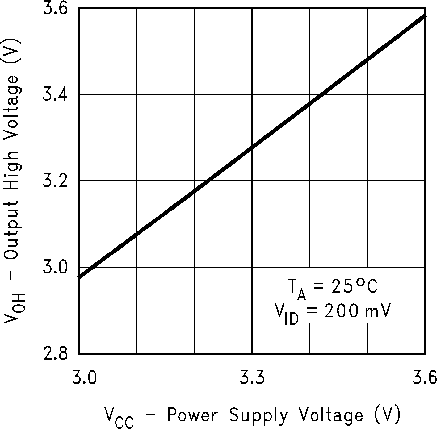 Figure 1. Output High Voltage vs Power Supply Voltage
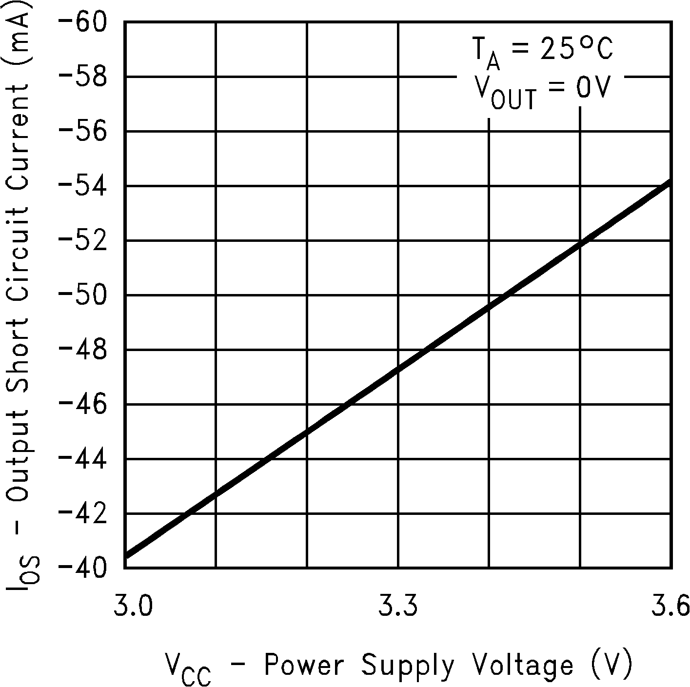 Figure 3. Output Short-Circuit Current vs Power Supply Voltage
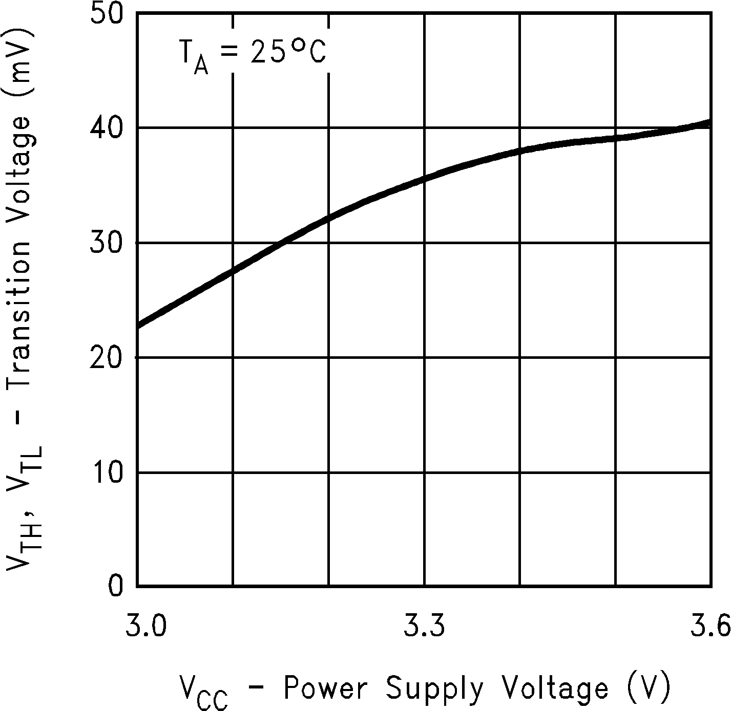 Figure 5. Differential Transition Voltage vs Power Supply Voltage
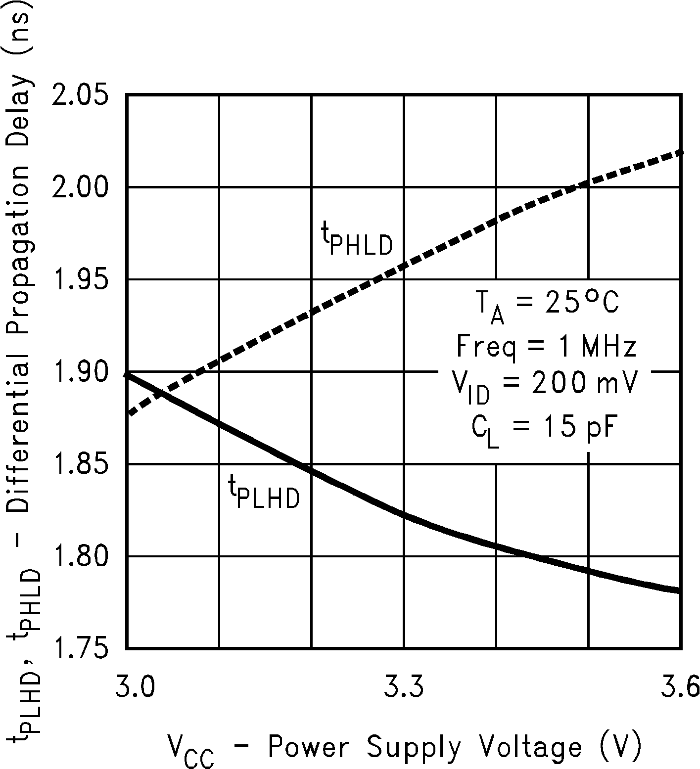 Figure 7. Differential Propagation Delay vs Power Supply Voltage
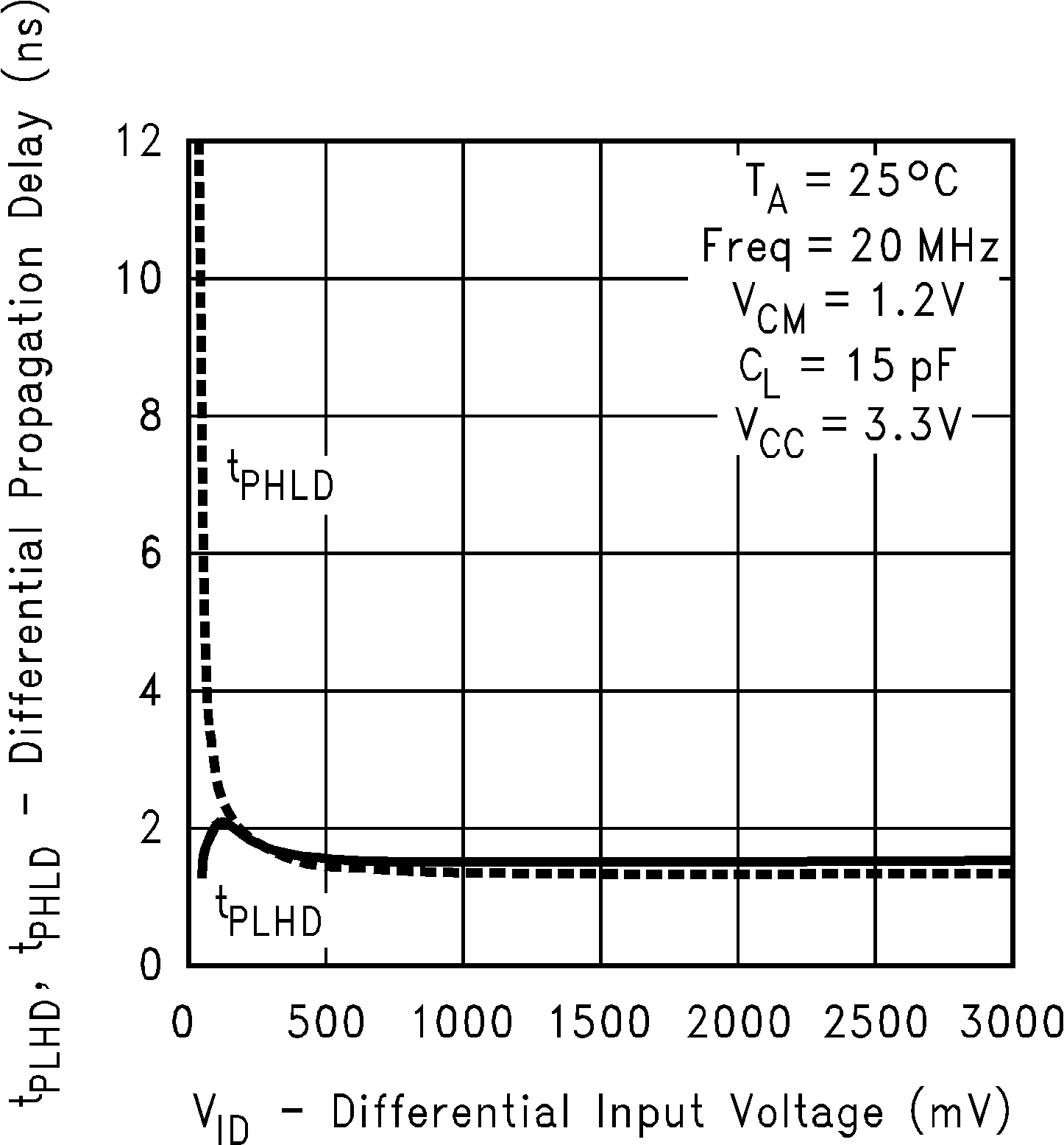 Figure 9. Differential Propagation Delay vs Differential Input Voltage
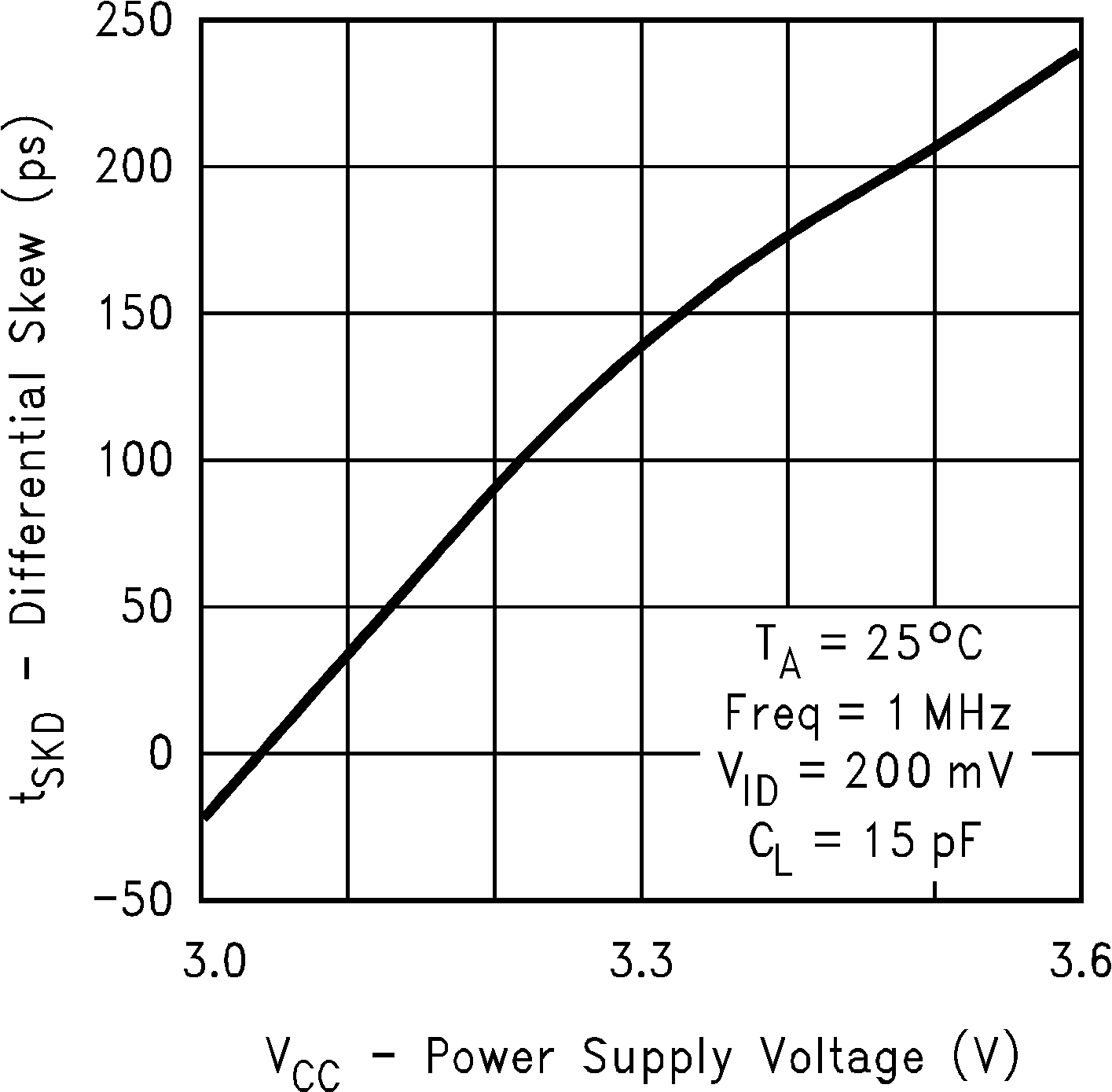 Figure 11. Differential Skew vs Power Supply Voltage
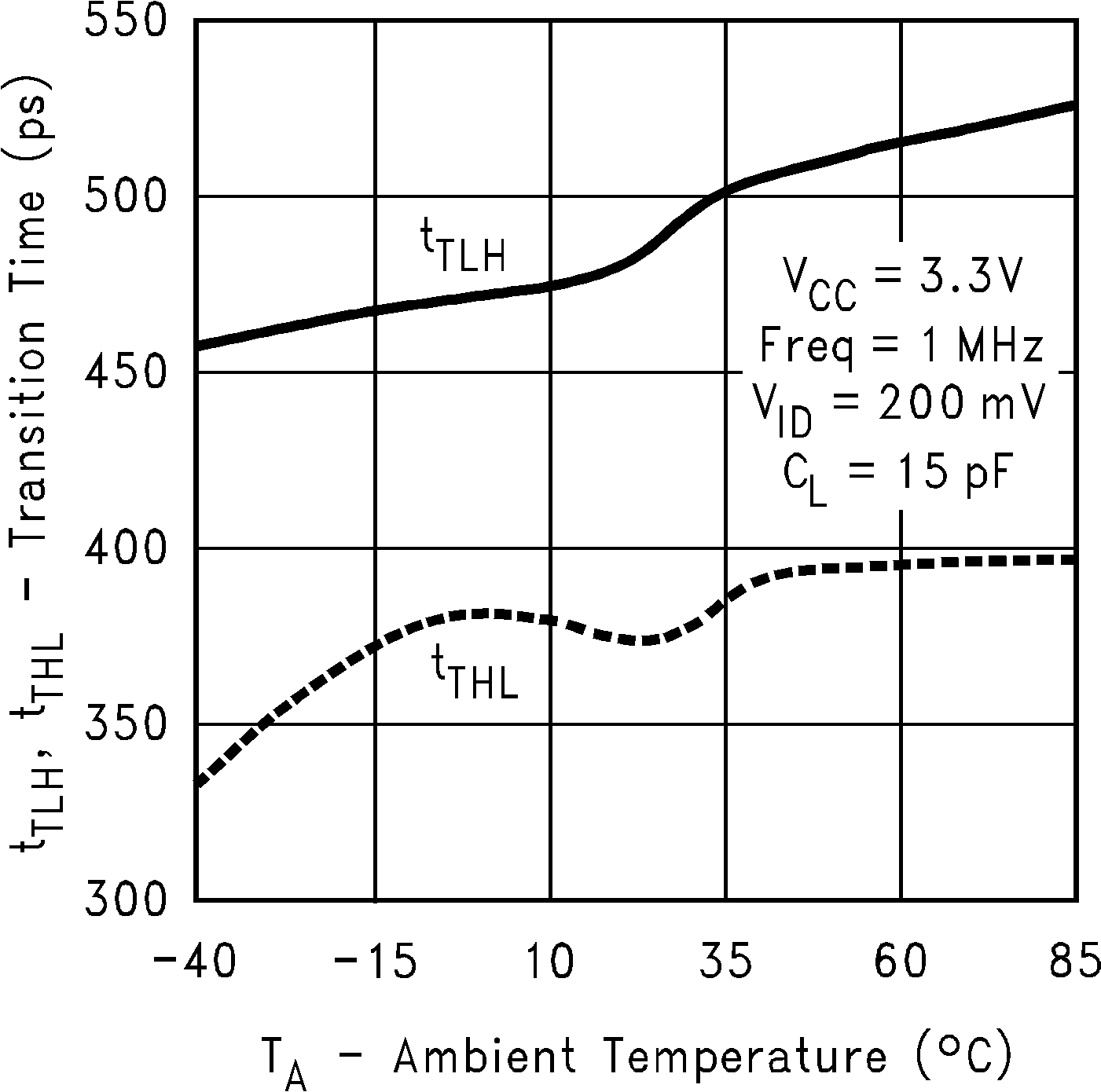
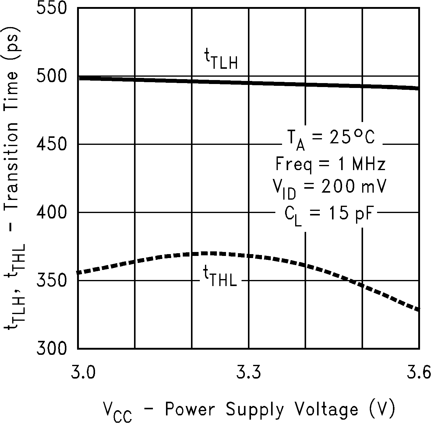 Figure 13. Transition Time vs Power Supply Voltage
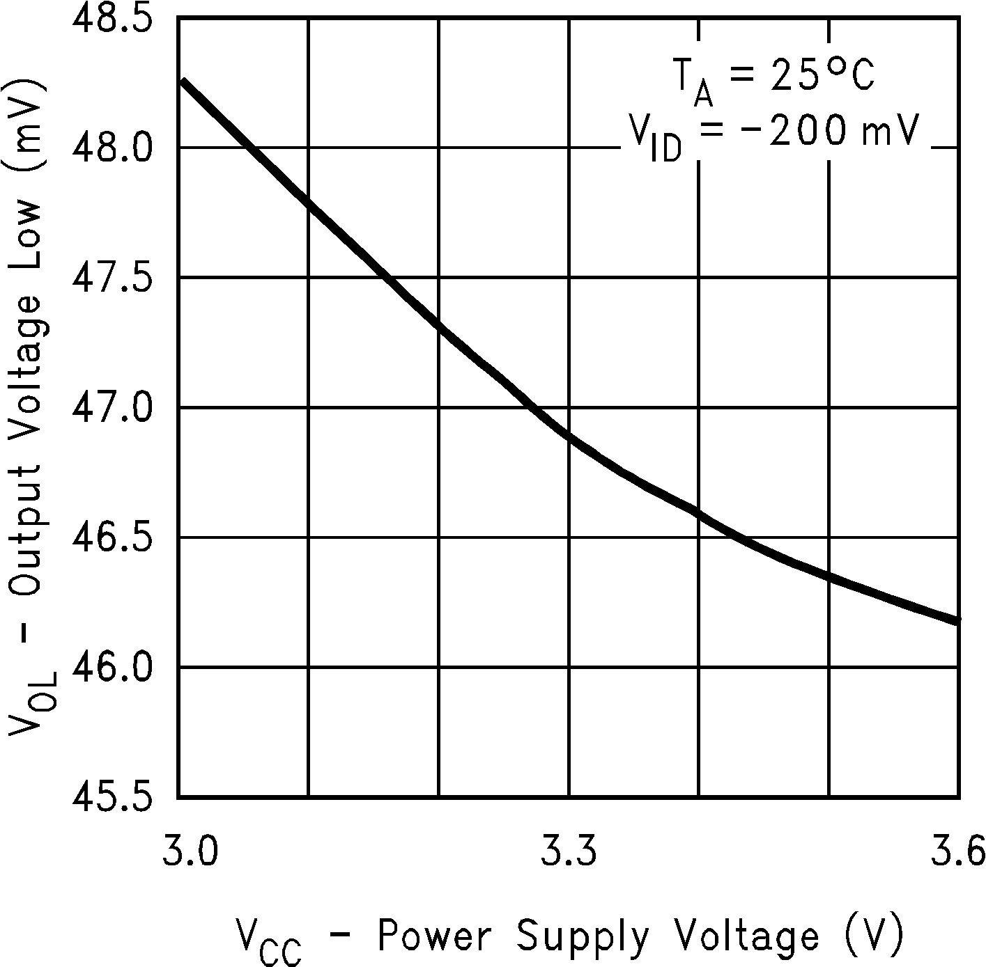 Figure 2. Output Low Voltage vs Power Supply Voltage
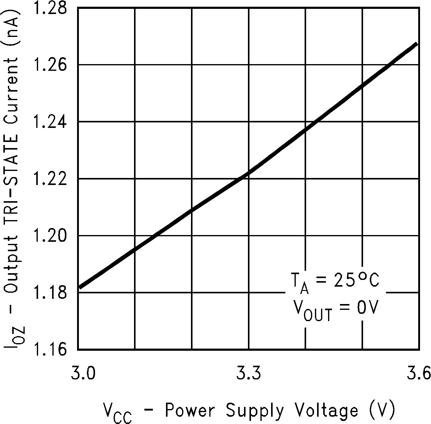 Figure 4. Output TRI-STATE Current vs Power Supply Voltage
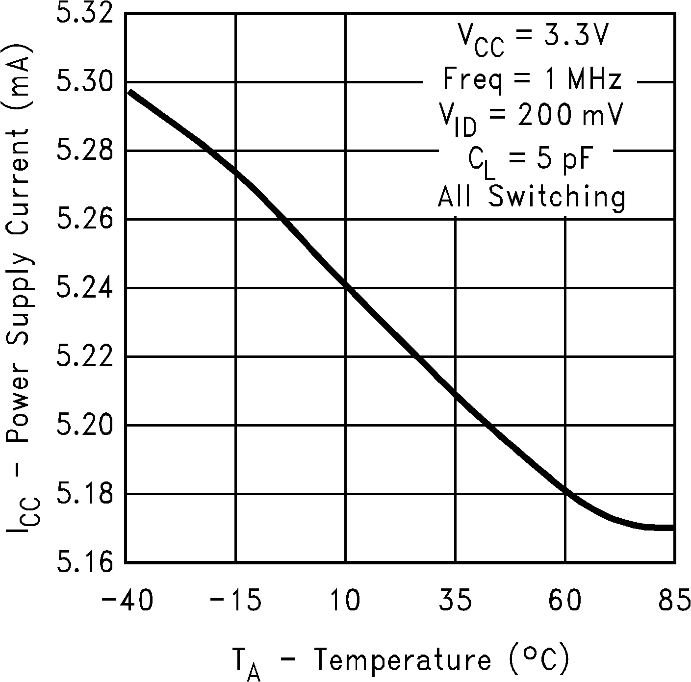 Figure 6. Power Supply Current vs Ambient Temperature
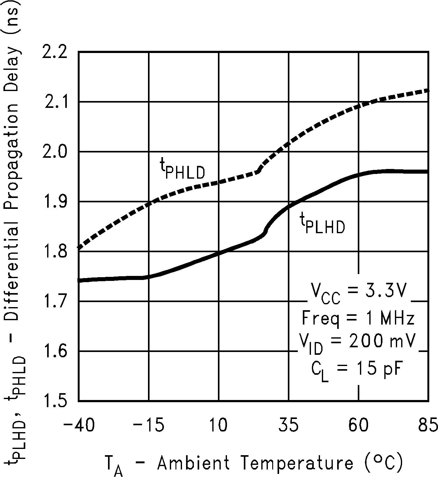 Figure 8. Differential Propagation Delay vs Ambient Temperature
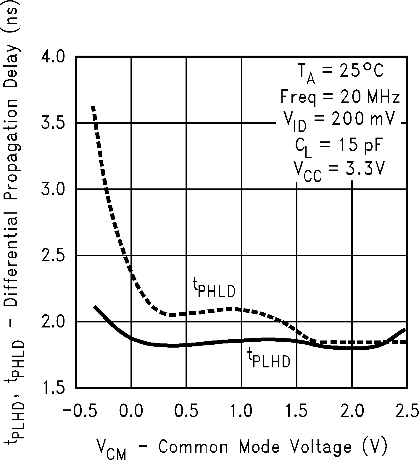 Figure 10. Differential Propagation Delay vs Common-Mode Voltage
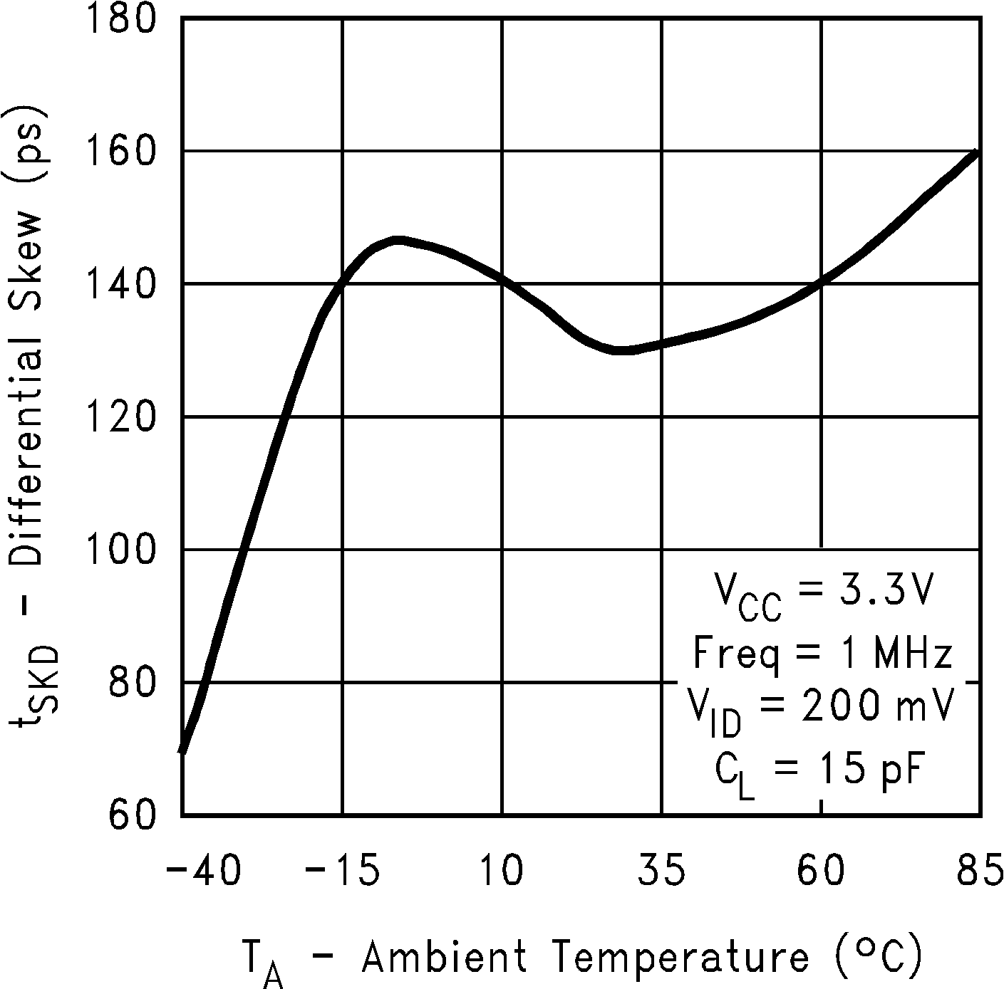 Figure 12. Differential Skew vs Ambient Temperature
