SNLS055J November 1999 – May 2016 DS90CF366 , DS90CF386
PRODUCTION DATA.
- 1 Features
- 2 Applications
- 3 Description
- 4 Revision History
- 5 Pin Configuration and Functions
- 6 Specifications
- 7 Detailed Description
- 8 Application and Implementation
- 9 Power Supply Recommendations
- 10Layout
- 11Device and Documentation Support
- 12Mechanical, Packaging, and Orderable Information
9 Power Supply Recommendations
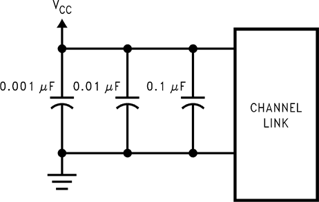
Proper power supply decoupling is important to ensure a stable power supply with minimal power supply noise. Bypassing capacitors are needed to reduce the impact of switching noise which could limit performance. For a conservative approach, three parallel-connected decoupling capacitors (multi-layered ceramic type in surface mount form factor) between each VCC (VCC, PLL VCC, LVDS VCC) and the ground plane(s) are recommended. The three capacitor values are 0.1 μF, 0.01 μF, and 0.001 μF. The preferred capacitor size is 0402. An example is shown in Figure 28. The designer should employ wide traces for power and ground and ensure each capacitor has its own via to the ground plane. This helps to reduce overall inductance with regards to power supply filtering. If board space is limiting the number of bypass capacitors, the PLL VCC should receive the most filtering. Next would be the LVDS VCC pins and finally the logic VCC pins.
 Figure 28. Recommended Bypass Capacitor Decoupling
 Configuration for VCC, PLL VCC, and LVDS VCC