ZHCSBO8A September 2013 – March 2014 DS125BR401A
PRODUCTION DATA.
- 1 特性
- 2 应用范围
- 3 说明
- 4 修订历史记录
- 5 Terminal Configuration and Functions
- 6 Specifications
- 7 Detailed Description
- 8 Applications and Implementation
- 9 Power Supply Recommendations
- 10Layout
- 11器件和文档支持
- 12机械封装和可订购信息
9 Power Supply Recommendations
Two approaches are recommended to ensure that the DS125BR401A is provided with an adequate power supply. First, the supply (VDD) and ground (GND) Terminals should be connected to power planes routed on adjacent layers of the printed circuit board. The layer thickness of the dielectric should be minimized so that the VDD and GND planes create a low inductance supply with distributed capacitance. Second, careful attention to supply bypassing through the proper use of bypass capacitors is required. A 0.1μF bypass capacitor should be connected to each VDD Terminal such that the capacitor is placed as close as possible to the DS125BR401A. Smaller body size capacitors can help facilitate proper component placement. Additionally, capacitor with capacitance in the range of 1 μF to 10 μF should be incorporated in the power supply bypassing design as well. These capacitors can be either tantalum or an ultra-low ESR ceramic.
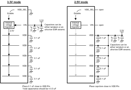
The DS125BR401A has an optional internal voltage regulator to provide the 2.5V supply to the device. In 3.3V mode operation, the VIN Terminal = 3.3V is used to supply power to the device. The internal regulator will provide the 2.5V to the VDD Terminals of the device and a 0.1uF cap is needed at each of the 5 VDD Terminals for power supply de-coupling (total capacitance should equal 0.5 uF). The VDD_SEL Terminal must be tied to GND to enable the internal regulator. In 2.5V mode operation, the VIN Terminal should be left open and 2.5V supply must be applied to the 5 VDD Terminals to power the device. The VDD_SEL Terminal must be left open (no connect) to disable the internal regulator.
 Figure 21. 3.3V or 2.5V Supply Connection Diagram