SLVSBN4C January 2013 – August 2016 DRV8839
PRODUCTION DATA.
8 Application and Implementation
NOTE
Information in the following applications sections is not part of the TI component specification, and TI does not warrant its accuracy or completeness. TI’s customers are responsible for determining suitability of components for their purposes. Customers should validate and test their design implementation to confirm system functionality.
8.1 Application Information
The DRV8839 is used in one control applications.
8.2 Typical Application
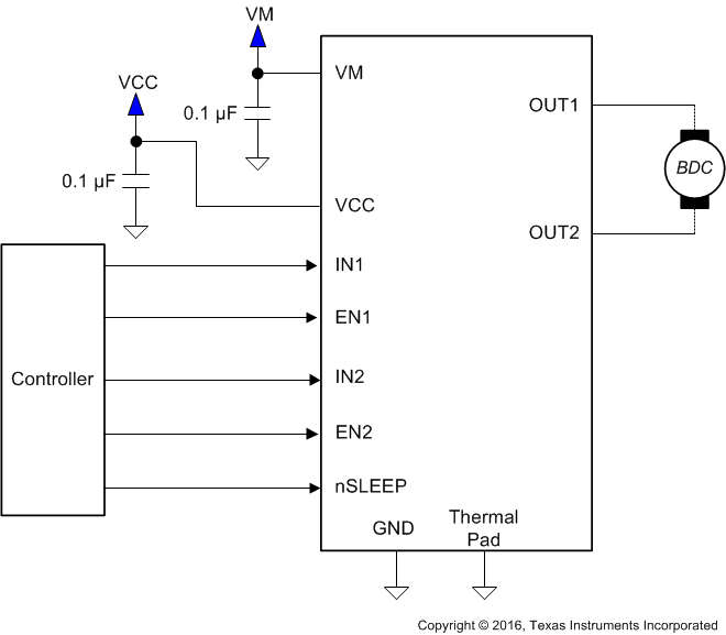
The following design is a common application of the DRV8839.
8.2.1 Design Requirements
The design requirements are shown in Table 6.
Table 6. Design Requirements
| DESIGN PARAMETER | REFERENCE | EXAMPLE VALUE |
|---|---|---|
| Motor voltage | VM | 5 V |
| Motor RMS current | IRMS | 0.3 A |
| Motor startup current | ISTART | 0.6 A |
8.2.2 Detailed Design Procedure
The following design procedure can be used to configure the DRV8839 in a brushed motor application.
8.2.2.1 Motor Voltage
The appropriate motor voltage depends on the ratings of the motor selected and the desired RPM. A higher voltage spins a brushed DC motor faster with the same PWM duty cycle applied to the power FETs. A higher voltage also increases the rate of current change through the inductive motor windings.
8.2.2.2 Low-Power Operation
When entering sleep mode, TI recommends setting all inputs as a logic low to minimize system power.
8.2.2.3 Application Curves
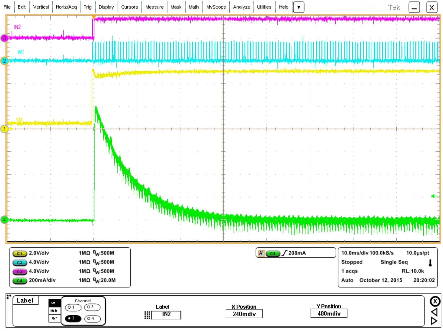
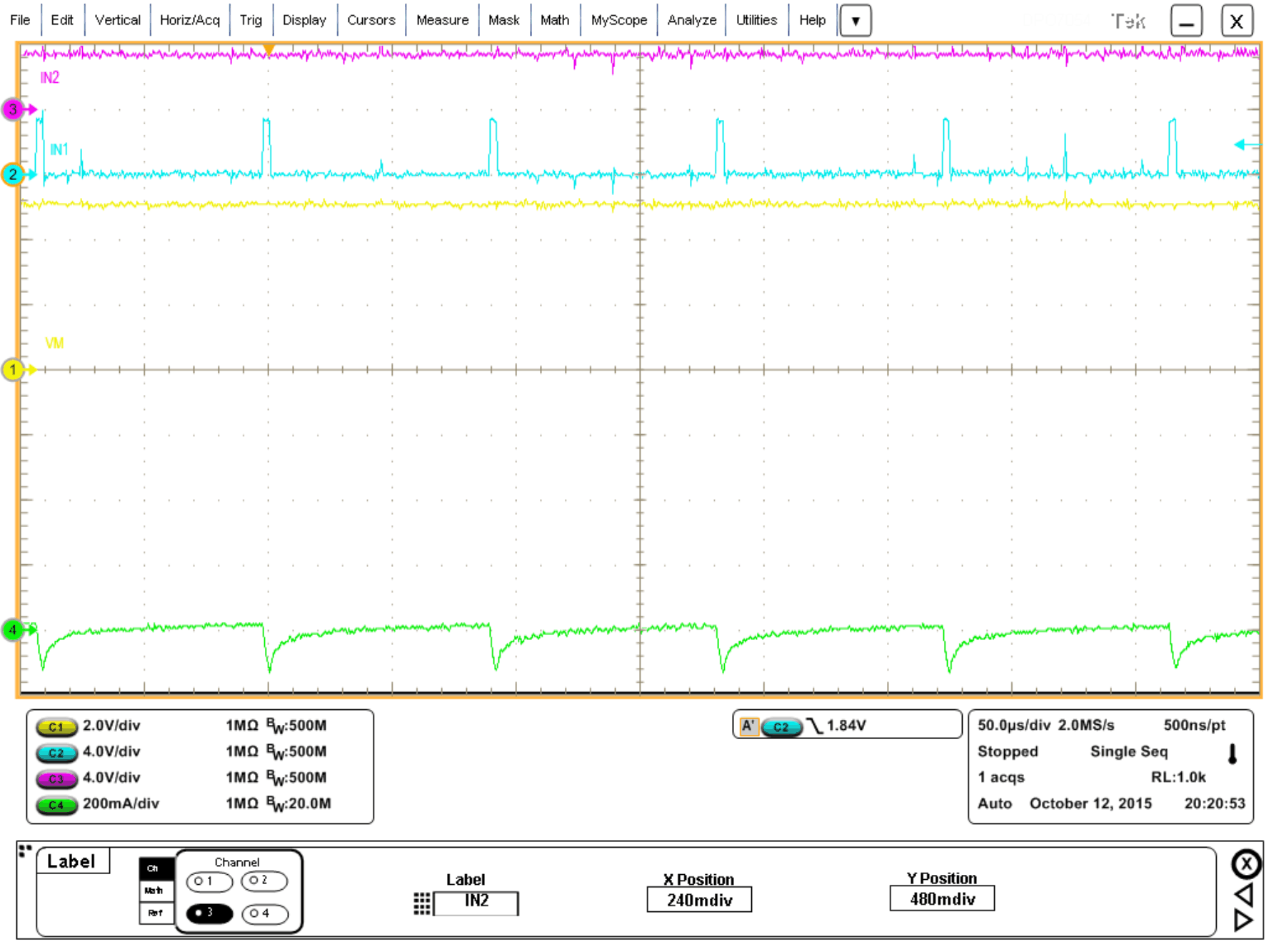
The following scope captures show a typical motor startup and running. Channel 1 is VM, Channel 2 is IN1, Channel 3 is IN2, and Channel 4 is motor current. the motor used is a NMB Technologies, PPN7PA12C1.
 Figure 10. Motor Startup With VCC = 3.3 V, VM = 5 V
 Figure 11. Motor Running With VCC = 3.3 V, VM = 5 V
