ZHCSA67F June   2012  – April 2021 DRV8837 , DRV8838

PRODUCTION DATA  

  1. 特性
  2. 应用范围
  3. 说明
  4. Revision History
  5. Pin Configuration and Functions
    1.     Pin Functions
    2. 5.1 Dapper Pin Functions
  6. Specifications
    1. 6.1 Absolute Maximum Ratings
    2. 6.2 ESD Ratings
    3. 6.3 Recommended Operating Conditions
    4. 6.4 Thermal Information
    5. 6.5 Electrical Characteristics
    6. 6.6 Timing Requirements
    7. 6.7 Typical Characteristics
  7. Detailed Description
    1. 7.1 Overview
    2. 7.2 Functional Block Diagram
    3. 7.3 Feature Description
      1. 7.3.1 Bridge Control
      2. 7.3.2 Independent Half-Bridge Control
      3. 7.3.3 Sleep Mode
      4. 7.3.4 Power Supplies and Input Pins
      5. 7.3.5 Protection Circuits
        1. 7.3.5.1 VCC Undervoltage Lockout
        2. 7.3.5.2 Overcurrent Protection (OCP)
        3. 7.3.5.3 Thermal Shutdown (TSD)
        4. 7.3.5.4 28
    4. 7.4 Device Functional Modes
      1.      Application and Implementation
        1. 8.1 Application Information
        2. 8.2 Typical Application
          1. 8.2.1 Design Requirements
          2. 8.2.2 Detailed Design Procedure
            1. 8.2.2.1 Motor Voltage
            2. 8.2.2.2 Low-Power Operation
          3. 8.2.3 Application Curves
  8. Power Supply Recommendations
    1. 8.1 Bulk Capacitance
  9. Layout
    1. 9.1 Layout Guidelines
    2. 9.2 Layout Example
    3. 9.3 Power Dissipation
  10. 10Device and Documentation Support
    1. 10.1 Documentation Support
      1. 10.1.1 Related Documentation
    2. 10.2 Related Links
    3. 10.3 Receiving Notification of Documentation Updates
    4. 10.4 Community Resources
    5. 10.5 Trademarks
      1.      Mechanical, Packaging, and Orderable Information

封装选项

机械数据 (封装 | 引脚)
散热焊盘机械数据 (封装 | 引脚)
订购信息

Power Dissipation

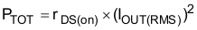
Power dissipation in the DRV883x family of devices is dominated by the power dissipated in the output FET resistance, or rDS(on). Use Equation 1 to estimate the average power dissipation when running a stepper motor.

Equation 1. GUID-C0878D78-D955-4108-AACA-259B8E50420D-low.gif

where

  • PTOT is the total power dissipation
  • rDS(on) is the resistance of the HS plus LS FETs
  • IOUT(RMS) is the rms or dc output current being supplied to the load

The maximum amount of power that can be dissipated in the device is dependent on ambient temperature and heatsinking.

Note:

The value of rDS(on) increases with temperature, so as the device heats, the power dissipation increases.

The DRV883x family of devices has thermal shutdown protection. If the die temperature exceeds approximately 150°C, the device is disabled until the temperature drops to a safe level.

Any tendency of the device to enter thermal shutdown is an indication of either excessive power dissipation, insufficient heatsinking, or too high an ambient temperature.