SLVS912J January 2009 – January 2016 DRV8821
PRODUCTION DATA.
- 1 Features
- 2 Applications
- 3 Description
- 4 Revision History
- 5 Pin Configuration and Functions
- 6 Specifications
- 7 Detailed Description
- 8 Application and Implementation
- 9 Power Supply Recommendations
- 10Layout
- 11Device and Documentation Support
- 12Mechanical, Packaging, and Orderable Information
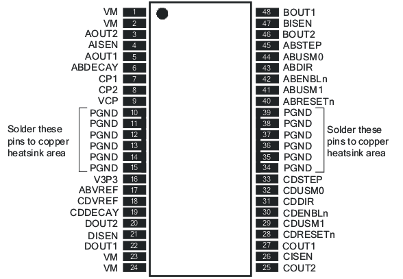
5 Pin Configuration and Functions
DCA Package
48-Pin HTSSOP
Top View

Pin Functions
| PIN | I/O(1) | DESCRIPTION | EXTERNAL COMPONENTS OR CONNECTIONS | |
|---|---|---|---|---|
| NAME | NO. | |||
| POWER AND GROUND | ||||
| VM (4 pins) |
1,2, 23, 24 |
— | Motor supply voltage (multiple pins) | Connect all VM pins together to motor supply voltage. Bypass each VM to GND with a 0.1-µF, 35-V ceramic capacitor. |
| V3P3 | 16 | — | 3.3 V regulator output | Bypass to GND with 0.47-μF, 6.3-V ceramic capacitor. |
| GND | 10-15, 34-39 |
— | Power ground (multiple pins) | Connect all PGND pins to GND and solder to copper heatsink areas. |
| CP1 | 7 | IO | Charge pump flying capacitor | Connect a 0.01-μF capacitor between CP1 and CP2 |
| CP2 | 8 | IO | ||
| VCP | 9 | IO | Charge pump storage capacitor | Connect a 0.1-μF, 16 V ceramic capacitor to VM |
| MOTOR AB | ||||
| ABSTEP | 45 | I | Motor AB step input | Rising edge causes the indexer to move one step. |
| ABDIR | 43 | I | Motor AB direction input | Level sets the direction of stepping. |
| ABUSM0 | 44 | I | Motor AB microstep mode 0 | USM0 and USM1 set the step mode - full step, half step, quarter step, or eight microsteps/step. |
| ABUSM1 | 41 | I | Motor AB microstep mode 1 | |
| ABENBLn | 42 | I | Motor AB enable input | Logic high to disable motor AB outputs, logic low to enable. |
| ABRESETn | 40 | I | Motor AB reset input | Active-low reset input initializes the indexer logic and disables the H-bridge outputs for motor AB. |
| ABDECAY | 6 | I | Motor AB decay mode | Logic low for slow decay mode, high for mixed decay. |
| ABVREF | 17 | I | Motor AB current set reference voltage | Sets current trip threshold. |
| AOUT1 | 5 | O | Bridge A output 1 | Connect to first coil of bipolar stepper motor AB, or DC motor winding. |
| AOUT2 | 3 | O | Bridge A output 2 | |
| AISEN | 4 | — | Bridge A current sense | Connect to current sense resistor for bridge A. |
| BOUT1 | 48 | O | Bridge B output 1 | Connect to second coil of bipolar stepper motor AB, or DC motor winding. |
| BOUT2 | 46 | O | Bridge B output 2 | |
| BISEN | 47 | — | Bridge B current sense | Connect to current sense resistor for bridge B. |
| MOTOR CD | ||||
| CDSTEP | 33 | I | Motor CD step input | Rising edge causes the indexer to move one step. |
| CDDIR | 31 | I | Motor CD direction input | Level sets the direction of stepping. |
| CDUSM0 | 32 | I | Motor CD microstep mode 0 | USM0 and USM1 set the step mode - full step, half step, quarter step, or eight microsteps/step. |
| CDUSM1 | 29 | I | Motor CD microstep mode 1 | |
| CDENBLn | 30 | I | Motor CD enable input | Logic high to disable motor CD outputs, logic low to enable. |
| CDRESETn | 28 | I | Motor CD reset input | Active-low reset input initializes the indexer logic and disables the H-bridge outputs for motor CD. |
| CDDECAY | 19 | I | Motor CD decay mode | Logic low for slow decay mode, high for mixed decay. |
| CDREF | 18 | I | Motor CD current set reference voltage | Sets current trip threshold. |
| COUT1 | 27 | O | Bridge C output 1 | Connect to first coil of bipolar stepper motor CD, or DC motor winding. |
| COUT2 | 25 | O | Bridge C output 2 | |
| CISEN | 26 | — | Bridge C current sense | Connect to current sense resistor for bridge C. |
| DOUT1 | 22 | O | Bridge D output 1 | Connect to second coil of bipolar stepper motor CD, or DC motor winding. |
| DOUT2 | 20 | O | Bridge D output 2 | |
| DISEN | 21 | — | Bridge D current sense | Connect to current sense resistor for bridge D. |
(1) Directions: i = input, O = output, OZ = 3-state output, OD = open-drain ouput, IO = input/ouput