ZHCSBL1B September 2013 – October 2014 DRV8816
PRODUCTION DATA.
11 Layout
11.1 Layout Guidelines
The printed circuit board (PCB) should use a heavy ground plane. For optimum electrical and thermal performance, the DRV8816 must be soldered directly onto the board. On the underside of the DRV8816 is a thermal pad, which provides a path for enhanced thermal dissipation. The thermal pad should be soldered directly to an exposed surface on the PCB. Thermal vias are used to transfer heat to other layers of the PCB.
The load supply pin, VBB, should be decoupled with an electrolytic capacitor (typically 100 μF) in parallel with a ceramic capacitor placed as close as possible to the device. The ceramic capacitors between VCP and VBB, connected to VREG, and between CP1 and CP2 should be as close to the pins of the device as possible, in order to minimize lead inductance.
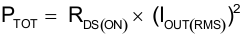
where
- PTOT is the total power dissipation.
- RDS(ON) is the resistance of the HS plus LS FETS.
- IOUT(RMS) is the RMS output current being applied to each winding.
The voltage rating for bulk capacitors should be higher than the operating voltage, to provide margin for cases when the motor transfers energy to the supply.
IOUT(RMS) is equal to approximately 0.7× the full-scale output current setting.
The maximum amount of power that can be dissipated in the device is dependent on ambient temperature and heatsinking.
Note that RDS(ON) increases with temperature, so as the device heats, the power dissipation increases.
11.1.1 Ground
A ground power plane should be located as close to DRV8816 as possible. The copper ground plane directly under the thermal pad makes a good location. This pad can then be connected to ground for this purpose.
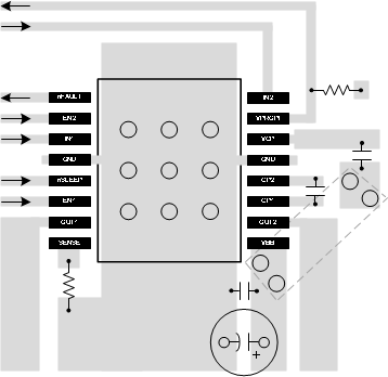
11.2 Layout Example
11.3 Thermal Protection
If the die temperature exceeds approximately 150°C, the device is disabled until the temperature drops to a safe level. Any tendency of the device to enter thermal shutdown is an indication of either excessive power dissipation, insufficient heatsinking, or too high an ambient temperature.