ZHCSDO0A March 2015 – May 2015 DRV8701
PRODUCTION DATA.
- 1 特性
- 2 应用
- 3 说明
- 4 修订历史记录
- 5 Pin Configuration and Functions
- 6 Specifications
-
7 Detailed Description
- 7.1 Overview
- 7.2 Functional Block Diagram
- 7.3
Feature Description
- 7.3.1 Bridge Control
- 7.3.2 Half-Bridge Operation
- 7.3.3 Current Regulation
- 7.3.4 Amplifier Output SO
- 7.3.5 PWM Motor Gate Drivers
- 7.3.6 IDRIVE Pin
- 7.3.7 Dead Time
- 7.3.8 Propagation Delay
- 7.3.9 Overcurrent VDS Monitor
- 7.3.10 Charge Pump
- 7.3.11 LDO Voltage Regulators
- 7.3.12 Gate Drive Clamp
- 7.3.13 Protection Circuits
- 7.3.14 Reverse Supply Protection
- 7.4 Device Functional Modes
- 8 Application and Implementation
- 9 Power Supply Recommendations
- 10Layout
- 11器件和文档支持
- 12机械、封装和可订购信息
10 Layout
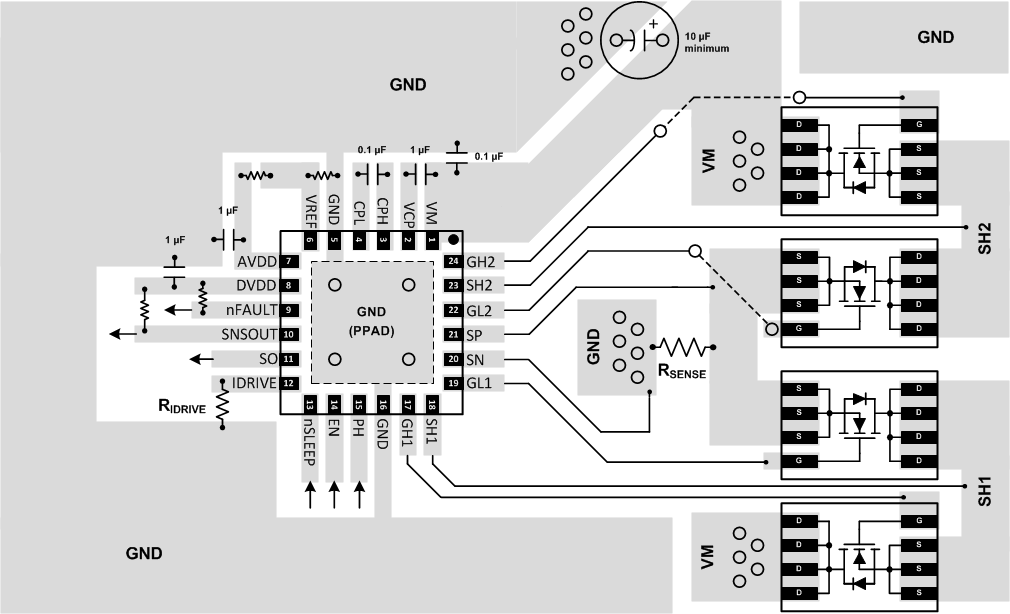
10.1 Layout Guidelines
Bypass the VM pin to GND using a low-ESR ceramic bypass capacitor with a recommended value of 0.1 µF rated for VM. Place this capacitor as close to the VM pin as possible with a thick trace or ground plane connection to the device GND pin.
Bypass the VM pin to ground using a bulk capacitor rated for VM. This component may be an electrolytic. This capacitance must be at least 10 µF. The bulk capacitor should be placed to minimize the distance of the high-current path through the external FETs. The connecting metal trace widths should be as wide as possible, and numerous vias should be used when connecting PCB layers. These practices minimize inductance and allow the bulk capacitor to deliver high current.
Place a low-ESR ceramic capacitor in between the CPL and CPH pins. The value for this component is 0.1 µF rated for VM. Place this component as close to the pins as possible.
Place a low-ESR ceramic capacitor in between the VM and VCP pins. The value for this component is 1 µF rated for 16 V. Place this component as close to the pins as possible.
Bypass AVDD and DVDD to ground with ceramic capacitors rated at 6.3 V. Place these bypassing capacitors as close to the pins as possible.
If desired, align the external NMOS FETs as shown in Figure 42 to facilitate layout. Route the SH2 and SH1 nets to the motor.
Use separate traces to connect the SP and SN pins to the RSENSE terminals.
10.2 Layout Example
 Figure 42. Layout Recommendation