ZHCSI91B November   2017  – July 2018 DRV8304

UNLESS OTHERWISE NOTED, this document contains PRODUCTION DATA.  

  1. 特性
  2. 应用
  3. 说明
    1.     简化原理图
  4. 修订历史记录
  5. Pin Configuration and Functions
    1.     Pin Functions
  6. Specifications
    1. 6.1 Absolute Maximum Ratings
    2. 6.2 ESD Ratings
    3. 6.3 Recommended Operating Conditions
    4. 6.4 Thermal Information
    5. 6.5 Electrical Characteristics
    6. 6.6 Timing Requirements
    7. 6.7 Typical Characteristics
  7. Detailed Description
    1. 7.1 Overview
    2. 7.2 Functional Block Diagram
    3. 7.3 Feature Description
      1. 7.3.1 3-Phase Smart Gate Drivers
        1. 7.3.1.1 PWM Control Modes
          1. 7.3.1.1.1 6x PWM Mode (PWM_MODE = 00b or MODE Pin Tied to AGND)
          2. 7.3.1.1.2 3x PWM Mode (PWM_MODE = 01b or MODE Pin = 47 kΩ to AGND)
          3. 7.3.1.1.3 1x PWM Mode (PWM_MODE = 10b or MODE Pin = Hi-Z)
          4. 7.3.1.1.4 Independent PWM Mode (PWM_MODE = 11b or MODE Pin Tied to DVDD)
        2. 7.3.1.2 Device Interface Modes
          1. 7.3.1.2.1 Serial Peripheral Interface (SPI)
          2. 7.3.1.2.2 Hardware Interface
        3. 7.3.1.3 Gate Driver Voltage Supplies
        4. 7.3.1.4 Smart Gate-Drive Architecture
          1. 7.3.1.4.1 IDRIVE: MOSFET Slew-Rate Control
          2. 7.3.1.4.2 TDRIVE: MOSFET Gate Drive Control
          3. 7.3.1.4.3 Gate Drive Clamp
          4. 7.3.1.4.4 Propagation Delay
          5. 7.3.1.4.5 MOSFET VDS Monitors
          6. 7.3.1.4.6 VDRAIN Sense Pin
      2. 7.3.2 DVDD Linear Voltage Regulator
      3. 7.3.3 Pin Diagrams
      4. 7.3.4 Low-Side Current-Shunt Amplifiers
        1. 7.3.4.1 Bidirectional Current Sense Operation
        2. 7.3.4.2 Unidirectional Current Sense Operation (SPI only)
        3. 7.3.4.3 Offset Calibration
      5. 7.3.5 Gate-Driver Protection Circuits
        1. 7.3.5.1 VM Supply Undervoltage Lockout (UVLO)
        2. 7.3.5.2 VCP Charge-Pump Undervoltage Lockout (CPUV)
        3. 7.3.5.3 MOSFET VDS Overcurrent Protection (VDS_OCP)
          1. 7.3.5.3.1 VDS Latched Shutdown (OCP_MODE = 00b)
          2. 7.3.5.3.2 VDS Automatic Retry (OCP_MODE = 01b)
          3. 7.3.5.3.3 VDS Report Only (OCP_MODE = 10b)
          4. 7.3.5.3.4 VDS Disabled (OCP_MODE = 11b)
        4. 7.3.5.4 VSENSE Overcurrent Protection (SEN_OCP)
          1. 7.3.5.4.1 VSENSE Latched Shutdown (OCP_MODE = 00b)
          2. 7.3.5.4.2 VSENSE Automatic Retry (OCP_MODE = 01b)
          3. 7.3.5.4.3 VSENSE Report Only (OCP_MODE = 10b)
          4. 7.3.5.4.4 VSENSE Disabled (OCP_MODE = 11b or DIS_SEN = 1b)
        5. 7.3.5.5 Gate Driver Fault (GDF)
        6. 7.3.5.6 Thermal Warning (OTW)
        7. 7.3.5.7 Thermal Shutdown (OTSD)
    4. 7.4 Device Functional Modes
      1. 7.4.1 Gate Driver Functional Modes
        1. 7.4.1.1 Sleep Mode
        2. 7.4.1.2 Operating Mode
        3. 7.4.1.3 Fault Reset (CLR_FLT or ENABLE Reset Pulse)
    5. 7.5 Programming
      1. 7.5.1 SPI Communication
        1. 7.5.1.1 SPI
          1. 7.5.1.1.1 SPI Format
    6. 7.6 Register Maps
      1. Table 1. DRV8304S Register Map
      2. 7.6.1     Status Registers (DRV8304S Only)
        1. 7.6.1.1 Fault Status Register 1 (Address = 0x00) [reset = 0x00]
          1. Table 11. Fault Status Register 1 Field Descriptions
        2. 7.6.1.2 Fault Status Register 2 (Address = 0x01) [reset = 0x00]
          1. Table 12. Fault Status Register 2 Field Descriptions
      3. 7.6.2     Control Registers (DRV8304S Only)
        1. 7.6.2.1 Driver Control Register (Address = 0x02) [reset = 0x00]
          1. Table 14. Driver Control Field Descriptions
        2. 7.6.2.2 Gate Drive HS Register (Address = 0x03) [reset = 0x377]
          1. Table 15. Gate Drive HS Field Descriptions
        3. 7.6.2.3 Gate Drive LS Register (Address = 0x04) [reset = 0x777]
          1. Table 16. Gate Drive LS Register Field Descriptions
        4. 7.6.2.4 OCP Control Register (Address = 0x05) [reset = 0x145]
          1. Table 17. OCP Control Field Descriptions
        5. 7.6.2.5 CSA Control Register (Address = 0x06) [reset = 0x283]
          1. Table 18. CSA Control Field Descriptions
  8. Application and Implementation
    1. 8.1 Application Information
    2. 8.2 Typical Application
      1. 8.2.1 Primary Application
        1. 8.2.1.1 Design Requirements
        2. 8.2.1.2 Detailed Design Procedure
          1. 8.2.1.2.1 External MOSFET Support
            1. 8.2.1.2.1.1 Example
          2. 8.2.1.2.2 IDRIVE Configuration
            1. 8.2.1.2.2.1 Example
          3. 8.2.1.2.3 VDS Overcurrent Monitor Configuration
            1. 8.2.1.2.3.1 Example
          4. 8.2.1.2.4 Sense-Amplifier Bidirectional Configuration
            1. 8.2.1.2.4.1 Example
        3. 8.2.1.3 Application Curves
      2. 8.2.2 Alternative Application
        1. 8.2.2.1 Design Requirements
        2. 8.2.2.2 Detailed Design Procedure
          1. 8.2.2.2.1 Sense-Amplifier Unidirectional Configuration
            1. 8.2.2.2.1.1 Example
  9. Power Supply Recommendations
    1. 9.1 Bulk Capacitance Sizing
  10. 10Layout
    1. 10.1 Layout Guidelines
    2. 10.2 Layout Example
  11. 11器件和文档支持
    1. 11.1 器件支持
      1. 11.1.1 器件命名规则
    2. 11.2 文档支持
      1. 11.2.1 相关文档
    3. 11.3 接收文档更新通知
    4. 11.4 社区资源
    5. 11.5 商标
    6. 11.6 静电放电警告
    7. 11.7 术语表
  12. 12机械、封装和可订购信息

封装选项

请参考 PDF 数据表获取器件具体的封装图。

机械数据 (封装 | 引脚)
  • RHA|40
散热焊盘机械数据 (封装 | 引脚)
订购信息

DVDD Linear Voltage Regulator

A 3.3-V, 30-mA linear regulator is integrated into the DRV8304 device and is available for use by external circuitry. This regulator can provide the supply voltage for a low-power microcontroller or other low-current supporting circuitry. The output of the DVDD regulator should be bypassed near the DVDD pin with a X5R or X7R, 1-µF, 6.3-V ceramic capacitor routed directly back to the adjacent AGND ground pin.

The DVDD nominal, no-load output voltage is 3.3 V. When the DVDD load current exceeds 30 mA, the regulator functions like a constant-current source. The output voltage drops significantly with a current load greater than 30 mA.
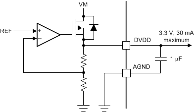
DRV8304 drv8304_dvdd_linear_regulator_block.gifFigure 24. DVDD Linear Regulator Block Diagram

Use Equation 1 to calculate the power dissipated in the device because of the DVDD linear regulator.

Equation 1. DRV8304 eq_01_power_slvsdj3.gif

For example, at VVM = 24 V, drawing 20 mA out of DVDD results in a power dissipation as shown in Equation 2.

Equation 2. DRV8304 eq_02_power_slvsdj3.gif