SNOSAY8F September 2007 – April 2015 DP83640
PRODUCTION DATA.
- 1Device Overview
- 2Revision History
-
3Pin Configuration and Functions
- 3.1 Pin Layout
- 3.2 Package Pin Assignments
- 3.3 Serial Management Interface (SMI)
- 3.4 MAC Data Interface
- 3.5 Clock Interface
- 3.6 LED Interface
- 3.7 IEEE 1588 Event/Trigger/Clock Interface
- 3.8 JTAG Interface
- 3.9 Reset and Power Down
- 3.10 Strap Options
- 3.11 10 Mb/s and 100 Mb/s PMD Interface
- 3.12 Power Supply Pins
- 4Specifications
-
5Detailed Description
- 5.1 Overview
- 5.2 Functional Block Diagram
- 5.3
Feature Description
- 5.3.1 Media Configuration
- 5.3.2 Auto-Negotiation
- 5.3.3 Auto-MDIX
- 5.3.4 LED Interface
- 5.3.5 Internal Loopback
- 5.3.6 Power Down/Interrupt
- 5.3.7 Energy Detect Mode
- 5.3.8 Link Diagnostic Capabilities
- 5.3.9 BIST
- 5.4 Device Functional Modes
- 5.5
Programming
- 5.5.1
Architecture
- 5.5.1.1 100BASE-TX Transmitter
- 5.5.1.2
100BASE-TX Receiver
- 5.5.1.2.1 Analog Front End
- 5.5.1.2.2 Digital Signal Processor
- 5.5.1.2.3 Signal Detect
- 5.5.1.2.4 MLT-3 to Binary Decoder
- 5.5.1.2.5 Clock Recovery Module
- 5.5.1.2.6 NRZI to NRZ Decoder
- 5.5.1.2.7 Serial-to-Parallel
- 5.5.1.2.8 Descrambler
- 5.5.1.2.9 Code-Group Alignment
- 5.5.1.2.10 4B/5B Decoder
- 5.5.1.2.11 100BASE-TX Link Integrity Monitor
- 5.5.1.2.12 Bad SSD Detection
- 5.5.1.3 100BASE-FX Operation
- 5.5.1.4
10BASE-T Transceiver Module
- 5.5.1.4.1 Operational Modes
- 5.5.1.4.2 Smart Squelch
- 5.5.1.4.3 Collision Detection and SQE
- 5.5.1.4.4 Carrier Sense
- 5.5.1.4.5 Normal Link Pulse Detection/Generation
- 5.5.1.4.6 Jabber Function
- 5.5.1.4.7 Automatic Link Polarity Detection and Correction
- 5.5.1.4.8 Transmit and Receive Filtering
- 5.5.1.4.9 Transmitter
- 5.5.1.4.10 Receiver
- 5.5.1
Architecture
- 5.6
Memory
- 5.6.1
Register Block
- 5.6.1.1
Register Definition
- 5.6.1.1.1 Basic Mode Control Register (BMCR)
- 5.6.1.1.2 Basic Mode Status Register (BMSR)
- 5.6.1.1.3 PHY Identifier Register #1 (PHYIDR1)
- 5.6.1.1.4 PHY Identifier Register #2 (PHYIDR2)
- 5.6.1.1.5 Auto-Negotiation Advertisement Register (ANAR)
- 5.6.1.1.6 Auto-Negotiation Link Partner Ability Register (ANLPAR) (BASE Page)
- 5.6.1.1.7 Auto-Negotiation Link Partner Ability Register (ANLPAR) (Next Page)
- 5.6.1.1.8 Auto-Negotiate Expansion Register (ANER)
- 5.6.1.1.9 Auto-Negotiation Next Page Transmit Register (ANNPTR)
- 5.6.1.1.10 PHY Status Register (PHYSTS)
- 5.6.1.1.11 MII Interrupt Control Register (MICR)
- 5.6.1.1.12 MII Interrupt Status and Event Control Register (MISR)
- 5.6.1.1.13 Page Select Register (PAGESEL)
- 5.6.1.2
Extended Registers - Page 0
- 5.6.1.2.1 False Carrier Sense Counter Register (FCSCR)
- 5.6.1.2.2 Receiver Error Counter Register (RECR)
- 5.6.1.2.3 100 Mb/s PCS Configuration and Status Register (PCSR)
- 5.6.1.2.4 RMII and Bypass Register (RBR)
- 5.6.1.2.5 LED Direct Control Register (LEDCR)
- 5.6.1.2.6 PHY Control Register (PHYCR)
- 5.6.1.2.7 10Base-T Status/Control Register (10BTSCR)
- 5.6.1.2.8 CD Test and BIST Extensions Register (CDCTRL1)
- 5.6.1.2.9 PHY Control Register 2 (PHYCR2)
- 5.6.1.2.10 Energy Detect Control (EDCR)
- 5.6.1.2.11 PHY Control Frames Configuration Register (PCFCR)
- 5.6.1.3 Test Registers - Page 1
- 5.6.1.4
Link Diagnostics Registers - Page 2
- 5.6.1.4.1 100 Mb Length Detect Register (LEN100_DET), Page 2
- 5.6.1.4.2 100 Mb Frequency Offset Indication Register (FREQ100), Page 2
- 5.6.1.4.3 TDR Control Register (TDR_CTRL), Page 2
- 5.6.1.4.4 TDR Window Register (TDR_WIN), Page 2
- 5.6.1.4.5 TDR Peak Register (TDR_PEAK), Page 2
- 5.6.1.4.6 TDR Threshold Register (TDR_THR), Page 2
- 5.6.1.4.7 Variance Control Register (VAR_CTRL), Page 2
- 5.6.1.4.8 Variance Data Register (VAR_DATA), Page 2
- 5.6.1.4.9 Link Quality Monitor Register (LQMR), Page 2
- 5.6.1.4.10 Link Quality Data Register (LQDR), Page 2
- 5.6.1.4.11 Link Quality Monitor Register 2 (LQMR2), Page 2
- 5.6.1.5
PTP 1588 Base Registers - Page 4
- 5.6.1.5.1 PTP Control Register (PTP_CTL), Page 4
- 5.6.1.5.2 PTP Time Data Register (PTP_TDR), Page 4
- 5.6.1.5.3 PTP Status Register (PTP_STS), Page 4
- 5.6.1.5.4 PTP Trigger Status Register (PTP_TSTS), Page 4
- 5.6.1.5.5 PTP Rate Low Register (PTP_RATEL), Page 4
- 5.6.1.5.6 PTP Rate High Register (PTP_RATEH), Page 4
- 5.6.1.5.7 PTP Read Checksum (PTP_RDCKSUM), Page 4
- 5.6.1.5.8 PTP Write Checksum (PTP_WRCKSUM), Page 4
- 5.6.1.5.9 PTP Transmit Timestamp Register (PTP_TXTS), Page 4
- 5.6.1.5.10 PTP Receive Timestamp Register (PTP_RXTS), Page 4
- 5.6.1.5.11 PTP Event Status Register (PTP_ESTS), Page 4
- 5.6.1.5.12 PTP Event Data Register (PTP_EDATA), Page 4
- 5.6.1.6
PTP 1588 Configuration Registers - Page 5
- 5.6.1.6.1 PTP Trigger Configuration Register (PTP_TRIG), Page 5
- 5.6.1.6.2 PTP Event Configuration Register (PTP_EVNT), Page 5
- 5.6.1.6.3 PTP Transmit Configuration Register 0 (PTP_TXCFG0), Page 5
- 5.6.1.6.4 PTP Transmit Configuration Register 1 (PTP_TXCFG1), Page 5
- 5.6.1.6.5 PHY Status Frame Configuration Register 0 (PSF_CFG0), Page 5
- 5.6.1.6.6 PTP Receive Configuration Register 0 (PTP_RXCFG0), Page 5,
- 5.6.1.6.7 PTP Receive Configuration Register 1 (PTP_RXCFG1), Page 5
- 5.6.1.6.8 PTP Receive Configuration Register 2 (PTP_RXCFG2), Page 5
- 5.6.1.6.9 PTP Receive Configuration Register 3 (PTP_RXCFG3), Page 5
- 5.6.1.6.10 PTP Receive Configuration Register 4 (PTP_RXCFG4), Page 5
- 5.6.1.6.11 PTP Temporary Rate Duration Low Register (PTP_TRDL), Page 5
- 5.6.1.6.12 PTP Temporary Rate Duration High Register (PTP_TRDH), Page 5
- 5.6.1.7
PTP 1588 Configuration Registers - Page 6
- 5.6.1.7.1 PTP Clock Output Control Register (PTP_COC), Page 6
- 5.6.1.7.2 PHY Status Frame Configuration Register 1 (PSF_CFG1), Page 6
- 5.6.1.7.3 PHY Status Frame Configuration Register 2 (PSF_CFG2), Page 6
- 5.6.1.7.4 PHY Status Frame Configuration Register 3 (PSF_CFG3), Page 6
- 5.6.1.7.5 PHY Status Frame Configuration Register 4 (PSF_CFG4), Page 6
- 5.6.1.7.6 PTP SFD Configuration Register (PTP_SFDCFG), Page 6
- 5.6.1.7.7 PTP Interrupt Control Register (PTP_INTCTL), Page 6
- 5.6.1.7.8 PTP Clock Source Register (PTP_CLKSRC), Page 6
- 5.6.1.7.9 PTP Ethernet Type Register (PTP_ETR), Page 6
- 5.6.1.7.10 PTP Offset Register (PTP_OFF), Page 6
- 5.6.1.7.11 PTP GPIO Monitor Register (PTP_GPIOMON), Page 6
- 5.6.1.7.12 PTP Receive Hash Register (PTP_RXHASH), Page 6
- 5.6.1.1
Register Definition
- 5.6.1
Register Block
-
6Application, Implementation, and Layout
- 6.1 Application Information
- 6.2 Typical Application
- 6.3 Layout
- 6.4 Power Supply Recommendations
- 7Device and Documentation Support
- 8Mechanical, Packaging, and Orderable Information
4 Specifications
4.1 Absolute Maximum Ratings(1)(2)
over operating free-air temperature range (unless otherwise noted)| MIN | MAX | UNIT | |
|---|---|---|---|
| Supply Voltage (VCC) | –0.5 | 4.2 | V |
| DC Input Voltage (VIN) | –0.5 to VCC + 0.5 | V | |
| DC Output Voltage (VOUT) | –0.5 to VCC + 0.5 | V | |
| Maximum Case Temperature for TA = 85 °C | 95 | °C | |
| Maximum Die Temperature (TJ) | 150 | °C | |
| Lead Temperature (TL) (Soldering, 10 s) |
260 | °C | |
| Storage temperature, Tstg | –65 | 150 | °C |
(1) Stresses beyond those listed under Absolute Maximum Ratings may cause permanent damage to the device. These are stress ratings only, and functional operation of the device at these or any other conditions beyond those indicated under Recommended Operating Conditions is not implied. Exposure to absolute-maximum-rated conditions for extended periods may affect device reliability.
(2) All voltage values are with respect to VSS, unless otherwise noted.
4.2 ESD Ratings
| VALUE | UNIT | |||
|---|---|---|---|---|
| V(ESD) | Electrostatic discharge(3) | Human body model (HBM), per ANSI/ESDA/JEDEC JS-001(1) | ±8000 | V |
| Charged device model (CDM), per JEDEC specification JESD22-C101(2) | ±1000 | |||
(1) JEDEC document JEP155 states that 500-V HBM allows safe manufacturing with a standard ESD control process.
(2) JEDEC document JEP157 states that 250-V CDM allows safe manufacturing with a standard ESD control process.
(3) RZAP = 1.5k, CZAP = 120 pF
4.3 Recommended Operating Conditions
over operating free-air temperature range (unless otherwise noted)| MIN | MAX | UNIT | |
|---|---|---|---|
| Analog Supply Voltage (VCC) | 3.3 ± 0.3 | V | |
| I/O Supply Voltage (VI/O) | 3.3 ± 10% or 2.5 ± 5% |
V | |
| Industrial Temperature (TI) | –40 | 85 | °C |
| Power Dissipation (PD) with VI/O = 3.3 V | 290 | mW | |
| Power Dissipation (PD) with VI/O = 2.5 V | 260 | mW |
4.4 Thermal Information
| THERMAL METRIC(1) | PT | UNIT | |
|---|---|---|---|
| 48 PINS | |||
| RθJA | Junction-to-ambient thermal resistance | 53.3(2) | °C/W |
| RθJC(top) | Junction-to-case (top) thermal resistance | 24.7 | |
(1) For more information about traditional and new thermal metrics, see the IC Package Thermal Metrics application report, SPRA953.
(2) No Airflow @ 1 W.
4.5 DC Specifications
| PIN TYPES |
PARAMETER | TEST CONDITIONS |
MIN | TYP | MAX | UNIT | |
|---|---|---|---|---|---|---|---|
| VIH | I I/O |
Input High Voltage | 2.0 | V | |||
| VIL | I I/O |
Input Low Voltage | VI/O = 3.3 V | 0.8 | V | ||
| VI/O = 2.5 V | 0.7 | V | |||||
| IIH | I I/O |
Input High Current | VIN = VI/O | 10 | µA | ||
| IIL | I I/O |
Input Low Current | VIN = GND | 10 | µA | ||
| VOL | O I/O |
Output Low Voltage | IOL = 4 mA | 0.4 | V | ||
| VOH | O I/O |
Output High Voltage | IOH = -4 mA | VI/O - 0.5 | V | ||
| IOZ | O I/O |
TRI-STATE Output Leakage Current | VOUT = VI/O or GND | –10 | 10 | µA | |
| VTPTD_100 | PMD Output Pair | 100M Transmit Voltage | 0.95 | 1 | 1.05 | V | |
| VTPTDsym | PMD Output Pair | 100M Transmit Voltage Symmetry | ±2% | ||||
| VTPTD_10 | PMD Output Pair | 10M Transmit Voltage | 2.2 | 2.5 | 2.8 | V | |
| VFXTD_100 | PMD Output Pair | FX 100M Transmit Voltage | 0.3 | 0.5 | 0.93 | V | |
| CIN1 | I | CMOS Input Capacitance | 8 | pF | |||
| COUT1 | O | CMOS Output Capacitance | 8 | pF | |||
| SDTHon | PMD Input Pair | 100BASE-TX Signal detect turnon threshold | 1000 | mV diff pk-pk | |||
| SDTHoff | PMD Input Pair | Signal detect turnoff threshold | 200 | mV diff pk-pk | |||
| VTH | PMD Input Pair | 10BASE-T Receive Threshold | 300 | 585 | mV | ||
| Idd100 | Supply | 100BASE-TX (Full Duplex) | VCC = 3.3 V, VI/O = 3.3 V, IOUT = 0 mA(1) | 88 | mA | ||
| VCC = 3.3 V, VI/O = 2.5 V, IOUT = 0 mA(1) | 84 | mA | |||||
| Idd10 | Supply | 10BASE-T (Full Duplex) | VCC = 3.3 V, VI/O = 3.3 V, IOUT = 0 mA(1) | 105 | mA | ||
| VCC = 3.3 V, VI/O = 2.5 V, IOUT = 0 mA(1) | 103 | mA | |||||
| Idd | Supply | Power Down Mode | CLK_OUT disabled | 10 | mA |
(1) For Idd measurements, outputs are not loaded
4.6 AC Timing Requirements
| PARAMETER | DESCRIPTION | NOTES | MIN | TYP | MAX | UNIT |
|---|---|---|---|---|---|---|
| POWER-UP TIMING (Refer to Figure 4-1) | ||||||
| T2.1.1 | Post Power Up Stabilization time prior to MDC preamble for register accesses(1) | MDIO is pulled high for 32-bit serial management initialization. | 167 | ms | ||
| T2.1.2 | Hardware Configuration Latch-in Time from power up(1) | Hardware Configuration Pins are described in Section 3. | 167 | |||
| T2.1.3 | Hardware Configuration pins transition to output drivers | 50 | ns | |||
| RESET TIMING (Refer to Figure 4-2) | ||||||
| T2.2.1 | Post RESET Stabilization time prior to MDC preamble for register accesses | MDIO is pulled high for 32-bit serial management initialization | 3 | µs | ||
| T2.2.2 | Hardware Configuration Latch-in Time from the Deassertion of RESET (either soft or hard) | Hardware Configuration Pins are described in Section 3 | 3 | µs | ||
| T2.2.3 | Hardware Configuration pins transition to output drivers(2) | 50 | ns | |||
| T2.2.4 | RESET pulse width | X1 Clock must be stable for at min. of 1 µs during RESET pulse low time. | 1 | µs | ||
| MII SERIAL MANAGEMENT TIMING (Refer to Figure 4-3) | ||||||
| T2.3.1 | MDC to MDIO (Output) Delay Time | 0 | 20 | ns | ||
| T2.3.2 | MDIO (Input) to MDC Setup Time | 10 | ||||
| T2.3.3 | MDIO (Input) to MDC Hold Time | 10 | ||||
| T2.3.4 | MDC Frequency | 2.5 | 25 | MHz | ||
| 100 Mb/s MII TRANSMIT TIMING (Refer to Figure 4-4) | ||||||
| T2.4.1 | TX_CLK High/Low Time | 100 Mb/s Normal mode | 16 | 20 | 24 | ns |
| T2.4.2 | TXD[3:0], TX_EN Data Setup to TX_CLK | 10 | ||||
| T2.4.3 | TXD[3:0], TX_EN Data Hold from TX_CLK | 0 | ||||
| 100 Mb/s MII RECEIVE TIMING (Refer to Figure 4-5) | ||||||
| T2.5.1 | RX_CLK High/Low Time(3) | 100 Mb/s Normal mode | 16 | 20 | 24 | ns |
| T2.5.2 | RX_CLK to RXD[3:0], RX_DV, RX_ER Delay | 10 | 30 | |||
| 100BASE-TX AND 100BASE-FX MII TRANSMIT PACKET LATENCY TIMING (Refer to Figure 4-6) | ||||||
| T2.6.1 | TX_CLK to PMD Output Pair Latency(5) | 100BASE-TX and 100BASE-FX modes IEEE 1588 One-Step Operation enabled(4) |
5 9 |
bits | ||
| 100BASE-TX AND 100BASE-FX MII TRANSMIT PACKET DEASSERTION TIMING (Refer to Figure 4-7) | ||||||
| T2.7.1 | TX_CLK to PMD Output Pair Deassertion(6) | 100BASE-TX and 100BASE-FX modes | 5 | bits | ||
| 100BASE-TX TRANSMIT TIMING (tR/F and Jitter) (Refer to Figure 4-8) | ||||||
| T2.8.1 | 100 Mb/s PMD Output Pair tR and tF(8) | 3 | 4 | 5 | ns | |
| 100 Mb/s tR and tF Mismatch(7) | 500 | ps | ||||
| T2.8.2 | 100 Mb/s PMD Output Pair Transmit Jitter | 1.4 | ns | |||
| 100BASE-TX AND 100BASE-FX MII RECEIVE PACKET LATENCY TIMING (Refer to Figure 4-9) | ||||||
| T2.9.1 | Carrier Sense ON Delay(9) | 100BASE-TX mode | 20 | bits(10) | ||
| 100BASE-FX mode | 10 | |||||
| T2.9.2 | Receive Data Latency(11)(12) | 100BASE-TX mode | 24 | |||
| 100BASE-FX mode | 14 | |||||
| 100BASE-TX AND 100BASE-FX MII RECEIVE PACKET DEASSERTION TIMING (Refer to Figure 4-10) | ||||||
| T2.10.1 | Carrier Sense OFF Delay(13) | 100BASE-TX mode | 24 | bits(14) | ||
| 100BASE-FX mode | 14 | |||||
| 10 Mb/s MII TRANSMIT TIMING(15) (Refer to Figure 4-11) | ||||||
| T2.11.1 | TX_CLK High/Low Time | 10 Mb/s MII mode | 190 | 200 | 210 | ns |
| T2.11.2 | TXD[3:0], TX_EN Data Setup to TX_CLK falling edge | 10 Mb/s MII mode | 25 | |||
| T2.11.3 | TXD[3:0], TX_EN Data Hold from TX_CLK rising edge | 10 Mb/s MII mode | 0 | |||
| 10 Mb/s MII RECEIVE TIMING (Refer to Figure 4-12) | ||||||
| T2.12.1 | RX_CLK High/Low Time(16) | 160 | 200 | 240 | ns | |
| T2.12.2 | RXD[3:0], RX_DV transition delay from RX_CLK rising edge | 10 Mb/s MII mode | 100 | |||
| T2.12.3 | RX_CLK rising edge delay from RXD[3:0], RX_DV valid data | 10 Mb/s MII mode | 100 | |||
| 10BASE-T MII TRANSMIT TIMING (START OF PACKET) (Refer to Figure 4-13) | ||||||
| T2.13.1 | Transmit Output Delay from the | 10 Mb/s MII mode | 3.5 | bits(17) | ||
| Falling Edge of TX_CLK | ||||||
| 10BASE-T MII TRANSMIT TIMING (END OF PACKET) (Refer to Figure 4-14) | ||||||
| T2.14.1 | End of Packet High Time | 250 | 300 | ns | ||
| (with '0' ending bit) | ||||||
| T2.14.2 | End of Packet High Time | 250 | 300 | ns | ||
| (with '1' ending bit) | ||||||
| 10BASE-T MII RECEIVE TIMING (START OF PACKET) (Refer to Figure 4-15) | ||||||
| T2.15.1 | Carrier Sense Turnon Delay (PMD Input Pair to CRS) | 630 | 1000 | ns | ||
| T2.15.2 | RX_DV Latency(18) | 10 | bits(19) | |||
| T2.15.3 | Receive Data Latency | Measurement shown from SFD | 8 | |||
| 10BASE-T MII RECEIVE TIMING (END OF PACKET) (Refer to Figure 4-16) | ||||||
| T2.16.1 | Carrier Sense Turnoff Delay | 1.0 | µs | |||
| 10 Mb/s HEARTBEAT TIMING (Refer to Figure 4-17) | ||||||
| T2.17.1 | CD Heartbeat Delay | All 10 Mb/s modes | 1200 | ns | ||
| T2.17.2 | CD Heartbeat Duration | All 10 Mb/s modes | 1000 | |||
| 10 Mb/s JABBER TIMING (Refer to Figure 4-18) | ||||||
| T2.18.1 | Jabber Activation Time | 85 | ms | |||
| T2.18.2 | Jabber Deactivation Time | 500 | ||||
| 10BASE-T NORMAL LINK PULSE TIMING(20) (Refer to Figure 4-19) | ||||||
| T2.19.1 | Pulse Width | 100 | ns | |||
| T2.19.2 | Pulse Period | 16 | ms | |||
| AUTO-NEGOTIATION FAST LINK PULSE (FLP) TIMING(21) (Refer to Figure 4-20) | ||||||
| T2.20.1 | Clock, Data Pulse Width | 100 | ns | |||
| T2.20.2 | Clock Pulse to Clock Pulse Period | 125 | µs | |||
| T2.20.3 | Clock Pulse to Data Pulse Period | Data = 1 | 62 | |||
| T2.20.4 | Burst Width | 2 | ms | |||
| T2.20.5 | FLP Burst to FLP Burst Period | 16 | ||||
| 100BASE-TX SIGNAL DETECT TIMING(22) (Refer to Figure 4-21) | ||||||
| T2.21.1 | SD Internal Turnon Time | 1 | ms | |||
| T2.21.2 | SD Internal Turnoff Time | Default operation Fast link-loss indication enabled(23) |
250 1.3 |
300 | µs µs |
|
| 100 Mb/s INTERNAL LOOPBACK TIMING (Refer to Figure 4-22) | ||||||
| T2.22.1 | TX_EN to RX_DV Loopback(24) | 100 Mb/s internal loopback mode(25) | 240 | ns | ||
| 10 Mb/s INTERNAL LOOPBACK TIMING (Refer to Figure 4-23) | ||||||
| T2.23.1 | TX_EN to RX_DV Loopback | 10 Mb/s internal loopback mode(26) | 2 | µs | ||
| RMII TRANSMIT TIMING (SLAVE MODE) (Refer to Figure 4-24) | ||||||
| T2.24.1 | X1 Clock Period | 50-MHz Reference Clock | 20 | ns | ||
| T2.24.2 | TXD[1:0], TX_EN, Data Setup to X1 rising edge | 4 | ||||
| T2.24.3 | TXD[1:0], TX_EN, Data Hold from X1 rising edge | 2 | ||||
| T2.24.4 | X1 Clock to PMD Output Pair Latency (100 Mb)(27) | 100BASE-TX or 100BASE-FX | 11 | bits | ||
| RMII TRANSMIT TIMING (MASTER MODE) (Refer to Figure 4-25) | ||||||
| T2.25.1 | RX_CLK, TX_CLK, CLK_OUT Period | 50-MHz Reference Clock | 20 | ns | ||
| T2.25.2 | TXD[1:0], TX_EN Data Setup to RX_CLK, TX_CLK, CLK_OUT rising edge | 4 | ||||
| T2.25.3 | TXD[1:0], TX_EN Data Hold from RX_CLK, TX_CLK, CLK_OUT rising edge | 2 | ||||
| T2.25.4 | RX_CLK, TX_CLK, CLK_OUT to PMD Output Pair Latency(28) | From RX_CLK rising edge to first bit of symbol | 11 | bits | ||
| RMII RECEIVE TIMING (SLAVE MODE)(29) (Refer to Figure 4-26) | ||||||
| T2.26.1 | X1 Clock Period | 50-MHz Reference Clock | 20 | ns | ||
| T2.26.2 | RXD[1:0], CRS_DV, and RX_ER output delay from X1 rising edge(30) | 2 | 14 | |||
| T2.26.3 | CRS ON delay(31) | 100BASE-TX mode | 18.5 | bits | ||
| 100BASE-FX mode | 9 | |||||
| T2.26.4 | CRS OFF delay (32) | 100BASE-TX mode | 27 | |||
| 100BASE-FX mode | 17 | |||||
| T2.26.5 | RXD[1:0] and RX_ER latency(33)(34)(35) | 100BASE-TX mode | 38 | |||
| 100BASE-FX mode | 27 | |||||
| RMII RECEIVE TIMING (MASTER MODE)(36) (Refer to Figure 4-27) | ||||||
| T2.27.1 | RX_CLK, TX_CLK, CLK_OUT Clock Period | 50-MHz Reference Clock | 20 | ns | ||
| T2.27.2 | RXD[1:0], CRS_DV, RX_DV and RX_ER output delay from RX_CLK, TX_CLK, CLK_OUT rising edge(37) | 2 | 14 | |||
| T2.27.3 | CRS ON delay(38) | 100BASE-TX mode | 18.5 | bits | ||
| 100BASE-FX mode | 9 | |||||
| T2.27.4 | CRS OFF delay (39) | 100BASE-TX mode | 27 | |||
| 100BASE-FX mode | 17 | |||||
| T2.27.5 | RXD[1:0] and RX_ER latency (40) | 100BASE-TX mode | 38 | |||
| 100BASE-FX mode | 27 | |||||
| RX_CLK TIMING (RMII MASTER MODE) (Refer to Figure 4-28) | ||||||
| T2.28.1 | RX_CLK High Time(41) | 12 | ns | |||
| T2.28.2 | RX_CLK Low Time(41) | 8 | ||||
| T2.28.3 | RX_CLK Period | 20 | ||||
| CLK_OUT TIMING (RMII SLAVE MODE) (Refer to Figure 4-29) | ||||||
| T2.29.1 | CLK_OUT High/Low Time | 10 | ns | |||
| T2.29.2 | CLK_OUT propagation delay | Relative to X1 | 8 | |||
| SINGLE CLOCK MII (SCMII) TRANSMIT TIMING (Refer to Figure 4-30) | ||||||
| T2.30.1 | X1 Clock Period | 25-MHz Reference Clock | 40 | ns | ||
| T2.30.2 | TXD[3:0], TX_EN Data Setup | To X1 rising edge | 4 | |||
| T2.30.3 | TXD[3:0], TX_EN Data Hold | From X1 rising edge | 2 | |||
| T2.30.4 | X1 Clock to PMD Output Pair Latency (100 Mb)(42) | 100BASE-TX or 100BASE-FX | 13 | bits | ||
| SINGLE CLOCK MII (SCMII) RECEIVE TIMING (Refer to Figure 4-31) | ||||||
| T2.31.1 | X1 Clock Period | 25-MHz Reference Clock(44) | 40 | ns | ||
| T2.31.2 | RXD[3:0], RX_DV and RX_ER output delay(43) | From X1 rising edge | 2 | 18 | ||
| T2.31.3 | CRS ON delay (45) | 100BASE-TX mode | 19 | bits | ||
| 100BASE-FX mode | 9 | |||||
| T2.31.4 | CRS OFF delay (46) | 100BASE-TX mode | 26 | |||
| 100BASE-FX mode | 16 | |||||
| T2.31.5 | RXD[3:0] and RX_ER latency(47) | 100BASE-TX mode | 56 | |||
| 100BASE-FX mode | 46 | |||||
| 100 Mb/s X1 TO TX_CLK TIMING (Refer to Figure 4-32) | ||||||
| T2.32.1 | X1 to TX_CLK delay(48) | 100 Mb/s Normal mode | 0 | 5 | ns | |
(1) In RMII Slave Mode, the minimum Post Power up Stabilization and Hardware Configuration Latch-in times are 84 ms.
(2) It is important to choose pullup and/or pulldown resistors for each of the hardware configuration pins that provide fast RC time constants in order to latch-in the proper value prior to the pin transitioning to an output driver.
(3) RX_CLK may be held low or high for a longer period of time during transition between reference and recovered clocks. Minimum high and low times will not be violated.
(4) For Normal mode, latency is determined by measuring the time from the first rising edge of TX_CLK occurring after the assertion of TX_EN to the first bit of the “J” code group as output from the PMD Output Pair. 1 bit time = 10 ns in 100 Mb/s mode.
(5) Enabling PHY Control Frames will add latency equal to 8 bits times the PCF_BUF_SIZE setting. For example if PCF_BUF_SIZE is set to 15, then the additional delay will be 15*8= 120 bits.
(6) Deassertion is determined by measuring the time from the first rising edge of TX_CLK occurring after the deassertion of TX_EN to the first bit of the "T" code group as output from the PMD Output Pair. 1 bit time = 10 ns in 100 Mb/s mode.
(7) Normal Mismatch is the difference between the maximum and minimum of all rise and fall times.
(8) Rise and fall times taken at 10% and 90% of the +1 or –1 amplitude.
(9) Carrier Sense On Delay is determined by measuring the time from the first bit of the “J” code group to the assertion of Carrier Sense.
(10) 1 bit time = 10 ns in 100 Mb/s mode.
(11) Enabling IEEE 1588 Receive Timestamp insertion will increase the Receive Data Latency by 40 bit times.
(12) Enabling PHY Status Frames will introduce variability in Receive Data Latency due to insertion of PHY Status Frames into the receive datapath.
(13) Carrier Sense Off Delay is determined by measuring the time from the first bit of the “T” code group to the deassertion of Carrier Sense.
(14) 1 bit time = 10 ns in 100 Mb/s mode.
(15) An attached Mac should drive the transmit signals using the positive edge of TX_CLK. As shown above, the MII signals are sampled on the falling edge of TX_CLK.
(16) RX_CLK may be held low for a longer period of time during transition between reference and recovered clocks. Minimum high and low times will not be violated.
(17) 1 bit time = 100 ns in 10 Mb/s mode.
(18) 10BASE-T RX_DV Latency is measured from first bit of preamble on the wire to the assertion of RX_DV.
(19) 1 bit time = 100 ns in 10 Mb/s mode.
(20) These specifications represent transmit timings.
(21) These specifications represent transmit timings.
(22) The signal amplitude on PMD Input Pair must be TP-PMD compliant.
(23) Fast Link-loss detect is enabled by setting the SD_CNFG[8] register bit to a 1.
(24) Due to the nature of the descrambler function, all 100BASE-TX Loopback modes will cause an initial “dead-time” of up to 550 µs during which time no data will be present at the receive MII outputs. The 100BASE-TX timing specified is based on device delays after the initial 550 µs “dead-time”.
(25) Measurement is made from the first rising edge of TX_CLK after assertion of TX_EN.
(26) Measurement is made from the first falling edge of TX_CLK after assertion of TX_EN.
(27) Latency measurement is made from the X1 rising edge to the first bit of symbol.
(28) Latency measurement is made from the RX_CLK rising edge to the first bit of symbol.
(29) Per the RMII Specification, output delays assume a 25-pF load.
(30) CRS_DV is asserted asynchronously in order to minimize latency of control signals through the PHY. CRS_DV may toggle synchronously at the end of the packet to indicate CRS deassertion.
(31) CRS ON delay is measured from the first bit of the JK symbol on the PMD Input Pair to initial assertion of CRS_DV.
(32) CRS OFF delay is measured from the first bit of the TR symbol on the PMD Input Pair to initial deassertion of CRS_DV.
(33) Receive Latency is measured from the first bit of the symbol pair on the PMD Input Pair. Typical values are with the Elasticity Buffer set to the default value (01).
(34) Enabling IEEE 1588 Receive Timestamp insertion will increase the Receive Data Latency by 40 bit times.
(35) Enabling PHY Status Frames will introduce variability in Receive Data Latency due to insertion of PHY Status Frames into the receive datapath.
(36) Per the RMII Specification, output delays assume a 25-pF load.
(37) CRS_DV is asserted asynchronously in order to minimize latency of control signals through the PHY. CRS_DV may toggle synchronously at the end of the packet to indicate CRS deassertion.
(38) CRS ON delay is measured from the first bit of the JK symbol on the PMD Input Pair to initial assertion of CRS_DV.
(39) CRS OFF delay is measured from the first bit of the TR symbol on the PMD Input Pair to initial deassertion of CRS_DV.
(40) Receive Latency is measured from the first bit of the symbol pair on the PMD Input Pair. Typical values are with the Elasticity Buffer set to the default value (01).
(41) The High Time and Low Tme will add up to 20 ns.
(42) Latency measurement is made from the X1 rising edge to the first bit of symbol.
(43) Output delays assume a 25-pF load.
(44) CRS is asserted and deasserted asynchronously relative to the reference clock.
(45) CRS ON delay is measured from the first bit of the JK symbol on the PMD Input Pair to assertion of CRS_DV.
(46) CRS OFF delay is measured from the first bit of the TR symbol on the PMD Input Pair to deassertion of CRS_DV.
(47) Receive Latency is measured from the first bit of the symbol pair on the PMD Input Pair. Typical values are with the Elasticity Buffer set to the default value (01).
(48) X1 to TX_CLK timing is provided to support devices that use X1 instead of TX_CLK as the reference for transmit MII data.
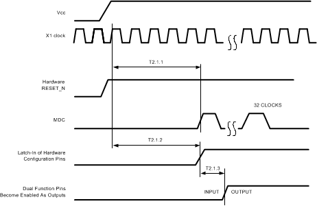 Figure 4-1 Power Up Timing
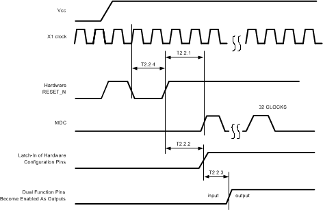 Figure 4-2 Reset Timing
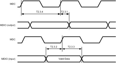 Figure 4-3 MII Serial Management Timing
 Figure 4-4 100 Mb/s MII Transmit Timing
 Figure 4-5 100 Mb/s MII Receive Timing
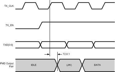 Figure 4-6 100BASE-TX and 100BASE-FX MII Transmit Packet Latency Timing
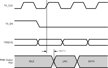 Figure 4-7 100BASE-TX and 100BASE-FX MII Transmit Packet Deassertion Timing
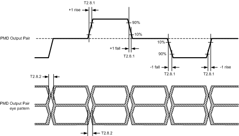 Figure 4-8 100BASE-TX Transmit Timing (tR/F and Jitter)
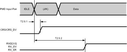 Figure 4-9 100BASE-TX and 100BASE-FX MII Receive Packet Latency Timing
 Figure 4-10 100BASE-TX and 100BASE-FX MII Receive Packet Deassertion Timing
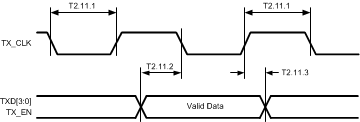 Figure 4-11 10 Mb/s MII Transmit Timing
 Figure 4-12 10 Mb/s MII Receive Timing
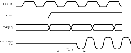 Figure 4-13 10BASE-T MII Transmit Timing (Start of Packet)
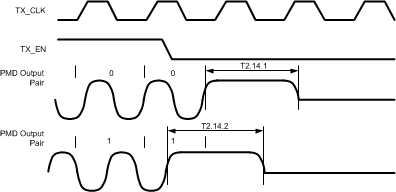 Figure 4-14 10BASE-T MII Transmit Timing (End of Packet)
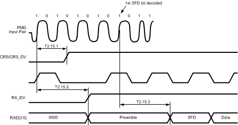 Figure 4-15 10BASE-T MII Receive Timing (Start of Packet)
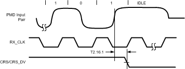 Figure 4-16 10BASE-T MII Receive Timing (End of Packet)
 Figure 4-17 10 Mb/s Heartbeat Timing
 Figure 4-18 10 Mb/s Jabber Timing
 Figure 4-19 10BASE-T Normal Link Pulse Timing
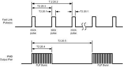 Figure 4-20 Auto-Negotiation Fast Link Pulse (FLP) Timing
 Figure 4-21 100BASE-TX Signal Detect Timing
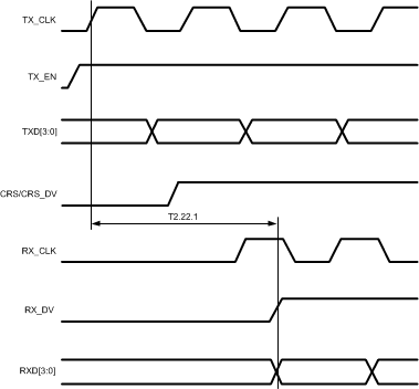 Figure 4-22 100 Mb/s Internal Loopback Timing
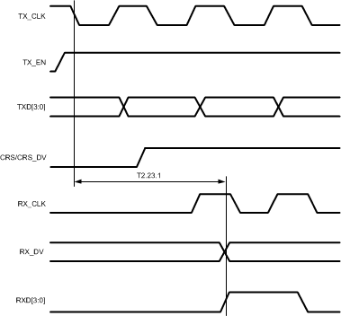 Figure 4-23 10 Mb/s Internal Loopback Timing
 Figure 4-24 RMII Transmit Timing (Slave Mode)
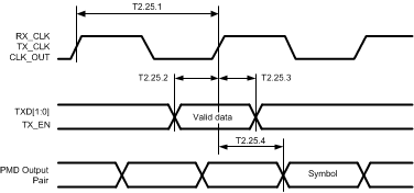 Figure 4-25 RMII Transmit Timing (Master Mode)
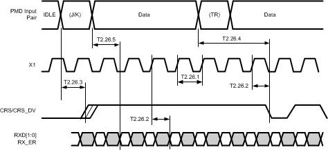 Figure 4-26 RMII Receive Timing (Slave Mode)
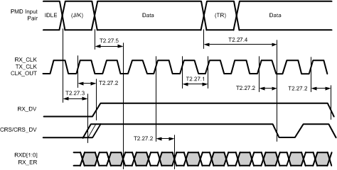 Figure 4-27 RMII Receive Timing (Master Mode)
 Figure 4-28 RX_CLK Timing (RMII Master Mode)
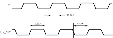 Figure 4-29 CLK_OUT Timing (RMII Slave Mode)
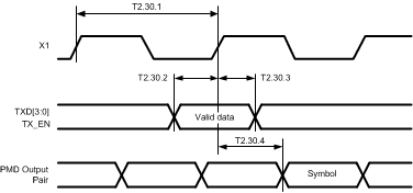 Figure 4-30 Single Clock MII (SCMII) Transmit Timing
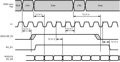 Figure 4-31 Single Clock MII (SCMII) Receive Timing
 Figure 4-32 100 Mb/s X1 to TX_CLK Timing