ZHCSIC5C June   2018  – August 2021 DLPC3479

PRODUCTION DATA  

  1. 特性
  2. 应用
  3. 说明
  4. Revision History
  5. Pin Configuration and Functions
  6. Specifications
    1. 6.1  Absolute Maximum Ratings
    2. 6.2  ESD Ratings
    3. 6.3  Recommended Operating Conditions
    4. 6.4  Thermal Information
    5. 6.5  Power Electrical Characteristics
    6. 6.6  Pin Electrical Characteristics
    7. 6.7  Internal Pullup and Pulldown Electrical Characteristics
    8. 6.8  DMD Sub-LVDS Interface Electrical Characteristics
    9. 6.9  DMD Low-Speed Interface Electrical Characteristics
    10. 6.10 System Oscillator Timing Requirements
    11. 6.11 Power Supply and Reset Timing Requirements
    12. 6.12 Parallel Interface Frame Timing Requirements
    13. 6.13 Parallel Interface General Timing Requirements
    14. 6.14 Flash Interface Timing Requirements
    15. 6.15 Other Timing Requirements
    16. 6.16 DMD Sub-LVDS Interface Switching Characteristics
    17. 6.17 DMD Parking Switching Characteristics
    18. 6.18 Chipset Component Usage Specification
  7. Detailed Description
    1. 7.1 Overview
    2. 7.2 Functional Block Diagram
    3. 7.3 Feature Description
      1. 7.3.1  Input Source Requirements
        1. 7.3.1.1 Supported Resolution and Frame Rates
        2. 7.3.1.2 3D Display
        3. 7.3.1.3 Parallel Interface
          1. 7.3.1.3.1 PDATA Bus – Parallel Interface Bit Mapping Modes
      2. 7.3.2  Pattern Display
        1. 7.3.2.1 External Pattern Mode
          1. 7.3.2.1.1 8-bit Monochrome Patterns
          2. 7.3.2.1.2 1-Bit Monochrome Patterns
        2. 7.3.2.2 Internal Pattern Mode
          1. 7.3.2.2.1 Free Running Mode
          2. 7.3.2.2.2 Trigger In Mode
      3. 7.3.3  Device Start-Up
      4. 7.3.4  SPI Flash
        1. 7.3.4.1 SPI Flash Interface
        2. 7.3.4.2 SPI Flash Programming
      5. 7.3.5  I2C Interface
      6. 7.3.6  Content Adaptive Illumination Control (CAIC)
      7. 7.3.7  Local Area Brightness Boost (LABB)
      8. 7.3.8  3D Glasses Operation
      9. 7.3.9  Test Point Support
      10. 7.3.10 DMD Interface
        1. 7.3.10.1 Sub-LVDS (HS) Interface
    4. 7.4 Device Functional Modes
    5. 7.5 Programming
  8. Application and Implementation
    1. 8.1 Application Information
    2. 8.2 Typical Application
      1. 8.2.1 Design Requirements
      2. 8.2.2 Detailed Design Procedure
      3. 8.2.3 Application Curve
  9. Power Supply Recommendations
    1. 9.1 PLL Design Considerations
    2. 9.2 System Power-Up and Power-Down Sequence
    3. 9.3 Power-Up Initialization Sequence
    4. 9.4 DMD Fast Park Control (PARKZ)
    5. 9.5 Hot Plug I/O Usage
  10. 10Layout
    1. 10.1 Layout Guidelines
      1. 10.1.1 PLL Power Layout
      2. 10.1.2 Reference Clock Layout
        1. 10.1.2.1 Recommended Crystal Oscillator Configuration
      3. 10.1.3 Unused Pins
      4. 10.1.4 DMD Control and Sub-LVDS Signals
      5. 10.1.5 Layer Changes
      6. 10.1.6 Stubs
      7. 10.1.7 Terminations
      8. 10.1.8 Routing Vias
      9. 10.1.9 Thermal Considerations
    2. 10.2 Layout Example
  11. 11Device and Documentation Support
    1. 11.1 Device Support
      1. 11.1.1 第三方产品免责声明
      2. 11.1.2 Device Nomenclature
        1. 11.1.2.1 Device Markings
      3. 11.1.3 Video Timing Parameter Definitions
    2. 11.2 Documentation Support
    3. 11.3 接收文档更新通知
    4. 11.4 支持资源
    5. 11.5 Trademarks
    6. 11.6 Electrostatic Discharge Caution
    7. 11.7 术语表
  12. 12Mechanical, Packaging, and Orderable Information

封装选项

机械数据 (封装 | 引脚)
散热焊盘机械数据 (封装 | 引脚)
订购信息

Reference Clock Layout

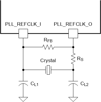
The DLPC34xx controller requires an external reference clock to feed the internal PLL. Use either a crystal or oscillator to supply this reference. The DLPC34xx reference clock must not exceed a frequency variation of ±200 ppm (including aging, temperature, and trim component variation).

Figure 10-2 shows the required discrete components when using a crystal.
GUID-86F1A110-6410-4A20-91D0-0C6903F65DA9-low.gif
CL = Crystal load capacitance (farads)
CL1 = 2 × (CL – Cstray_pll_refclk_i)
CL2 = 2 × (CL – Cstray_pll_refclk_o)
where:
  • Cstray_pll_refclk_i = Sum of package and PCB stray capacitance at the crystal pin associated with the controller pin pll_refclk_i.
  • Cstray_pll_refclk_o = Sum of package and PCB stray capacitance at the crystal pin associated with the controller pin pll_refclk_o.
Figure 10-2 Required Discrete Components