ZHCSQT7E October   2001  – July 2022 DCR010503 , DCR010505 , DCR011203 , DCR011205 , DCR012403 , DCR012405

PRODUCTION DATA  

  1. 特性
  2. 应用
  3. 说明
  4. Revision History
  5. Device Comparison Table
  6. Pin Configuration and Functions
  7. Specifications
    1. 7.1 Absolute Maximum Ratings
    2. 7.2 ESD Ratings
    3. 7.3 Recommended Operating Conditions
    4. 7.4 Thermal Information
    5. 7.5 Electrical Characteristics
    6. 7.6 Typical Characteristics
  8. Detailed Description
    1. 8.1 Overview
    2. 8.2 Functional Block Diagram
    3. 8.3 Feature Description
      1. 8.3.1  Isolation
        1. 8.3.1.1 Operation or Functional Isolation
        2. 8.3.1.2 Basic or Enhanced Isolation
        3. 8.3.1.3 Working Voltage
        4. 8.3.1.4 Isolation Voltage Rating
        5. 8.3.1.5 Repeated High-Voltage Isolation Testing
      2. 8.3.2  Power Stage
      3. 8.3.3  Rectification
      4. 8.3.4  Regulator
      5. 8.3.5  Oscillator and Watchdog
      6. 8.3.6  ERROR Flag
      7. 8.3.7  Synchronization
      8. 8.3.8  Construction
      9. 8.3.9  Thermal Considerations
      10. 8.3.10 Decoupling – Ripple Reduction
    4. 8.4 Device Functional Modes
      1. 8.4.1 Device Disable and Enable
      2. 8.4.2 Regulated Output Disable and Enable
  9. Application and Implementation
    1. 9.1 Application Information
      1. 9.1.1 DCR01 Single Voltage Output
      2. 9.1.2 Generating Two Positive Output Voltages
      3. 9.1.3 Generation of Dual Polarity Voltages from Two Self-Synchronized DCR01s
    2. 9.2 Typical Application
      1. 9.2.1 Design Requirements
      2. 9.2.2 Detailed Design Procedure
        1. 9.2.2.1 Input Capacitor
        2. 9.2.2.2 Output Capacitor
        3. 9.2.2.3 Filter Capacitor
        4. 9.2.2.4 ERROR Flag
      3. 9.2.3 Application Curves
  10. 10Power Supply Recommendations
  11. 11Layout
    1. 11.1 Layout Guidelines
    2. 11.2 Layout Examples
  12. 12Device and Documentation Support
    1. 12.1 接收文档更新通知
    2. 12.2 支持资源
    3. 12.3 Trademarks
    4. 12.4 Electrostatic Discharge Caution
    5. 12.5 术语表
  13. 13Mechanical, Packaging, and Orderable Information

封装选项

机械数据 (封装 | 引脚)
散热焊盘机械数据 (封装 | 引脚)
订购信息

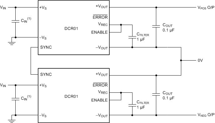
Generation of Dual Polarity Voltages from Two Self-Synchronized DCR01s

Two DCR01s can be configured to produce a dual polarity supply (that is, ±5 V); the circuit must be connected as shown in Figure 9-3.

Observe that both devices are producing a positive regulated output; therefore the ERROR, ENABLE, and VREC are all relative to the –VOUT pin of that particular device and must not be directly connected together, or in the case of the negative output device, connected to the common 0-V output.
GUID-DFBA9CC6-B6D8-41ED-A1BF-04722D86AEFF-low.gif
CIN = 2.2 μF for 5-V input devices and 0.47 μF for 12-V and 24-V input devices. Low-ESR, ceramic capacitors are required.
Figure 9-3 Dual Polarity Voltage Generation