| STATIC CHARACTERISTICS |
| BVDSS |
Drain-to-Source Voltage |
VGS = 0 V, ID = 250 μA |
100 |
|
|
V |
| IDSS |
Drain-to-Source Leakage Current |
VGS = 0 V, VDS = 80 V |
|
|
1 |
μA |
| IGSS |
Gate-to-Source Leakage Current |
VDS = 0 V, VGS = 20 V |
|
|
100 |
nA |
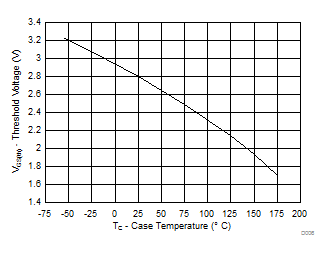
| VGS(th) |
Gate-to-Source Threshold Voltage |
VDS = VGS, ID = 250 μA |
2.4 |
2.8 |
3.4 |
V |
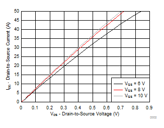
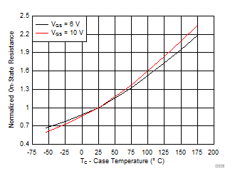
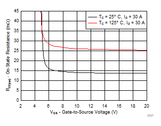
| RDS(on) |
Drain-to-Source On-Resistance |
VGS = 6 V, ID = 30 A |
|
16.3 |
20.0 |
mΩ |
| VGS = 10 V, ID = 30 A |
|
13.7 |
16.5 |
mΩ |
| gƒs |
Transconductance |
VDS = 10 V, ID = 30 A |
|
80 |
|
S |
| DYNAMIC CHARACTERISTICS |
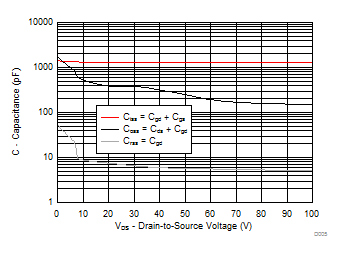
| Ciss |
Input Capacitance |
VGS = 0 V, VDS = 50 V, ƒ = 1 MHz |
|
1290 |
1670 |
pF |
| Coss |
Output Capacitance |
|
257 |
334 |
pF |
| Crss |
Reverse Transfer Capacitance |
|
5.7 |
7.4 |
pF |
| RG |
Series Gate Resistance |
|
|
1.1 |
2.2 |
Ω |
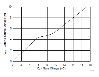
| Qg |
Gate Charge Total (10 V) |
VDS = 50 V, ID = 30 A |
|
17.1 |
22.2 |
nC |
| Qgd |
Gate Charge Gate-to-Drain |
|
3.2 |
|
nC |
| Qgs |
Gate Charge Gate-to-Source |
|
5.1 |
|
nC |
| Qg(th) |
Gate Charge at Vth |
|
3.3 |
|
nC |
| Qoss |
Output Charge |
VDS = 50 V, VGS = 0 V |
|
44 |
|
nC |
| td(on) |
Turn On Delay Time |
VDS = 50 V, VGS = 10 V,
IDS = 30 A, RG = 0 Ω |
|
6 |
|
ns |
| tr |
Rise Time |
|
2 |
|
ns |
| td(off) |
Turn Off Delay Time |
|
9 |
|
ns |
| tƒ |
Fall Time |
|
1 |
|
ns |
| DIODE CHARACTERISTICS |
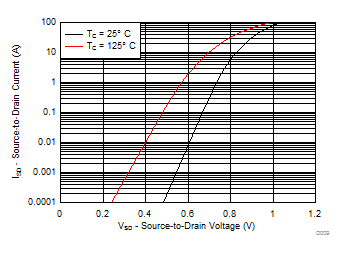
| VSD |
Diode Forward Voltage |
ISD = 30 A, VGS = 0 V |
|
0.9 |
1.1 |
V |
| Qrr |
Reverse Recovery Charge |
VDS= 50 V, IF = 30 A,
di/dt = 300 A/μs |
|
195 |
|
nC |
| trr |
Reverse Recovery Time |
|
72 |
|
ns |
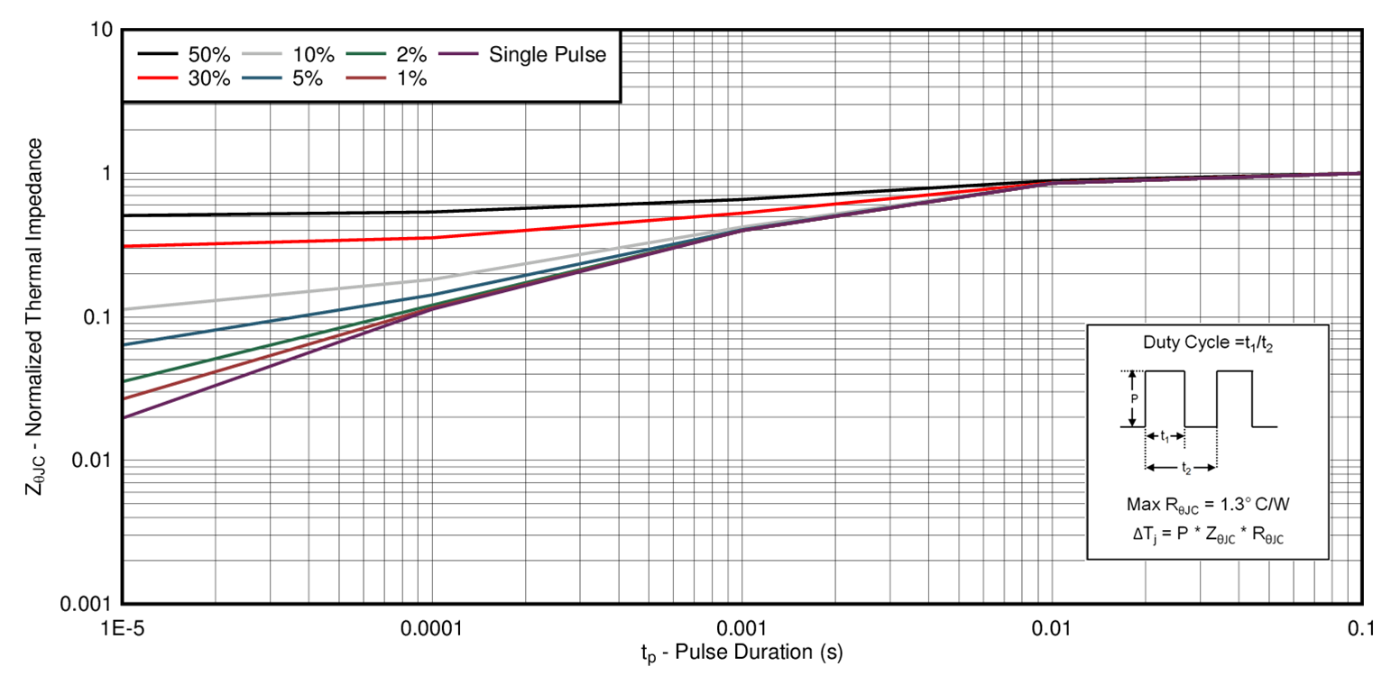 Figure 1. Transient Thermal Impedance