ZHCSG99 April 2017 CDCS504-Q1
PRODUCTION DATA.
8 Detailed Description
8.1 Overview
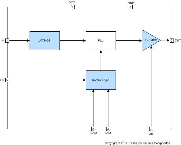
The CDCS504-Q1 is a LVCMOS clock buffer (x1 mode) or quadrupler (x4 mode). It integrates an internal PLL and generates a LVCMOS clock frequency range from 2 MHz to 108 MHz.
8.2 Functional Block Diagram

8.3 Feature Description
The CDCS504-Q1 is qualified for automotive applications with AEC-Q100 test, which could support wide temperature range from –40°C to 105°C. The device is easy to use, only need single 3.3-V power supply. The output enable or disable mode, along with frequency multiplication, could be controlled by external controls pins.
8.4 Device Functional Modes
When pin 7 OE is in low, the CDCS504-Q1 outputs 3-state. When pin 7 OE is set in high, the device would output clocks, output frequency depends on pin 5 FS status. FS = high enables frequency ×4 mode. FS= low makes output frequency equal to input frequency. If no input clock is provided, it is recommended to set OE=low in order to avoid random clock pulses from the internal PLL at the outputs.
Table 1. Function Table
| OE | FS | fOUT/fIN | fOUT at fin = 27 MHz |
|---|---|---|---|
| 0 | x | x | 3-state |
| 1 | 0 | 1 | 27 MHz |
| 1 | 1 | 4 | 108 MHz |