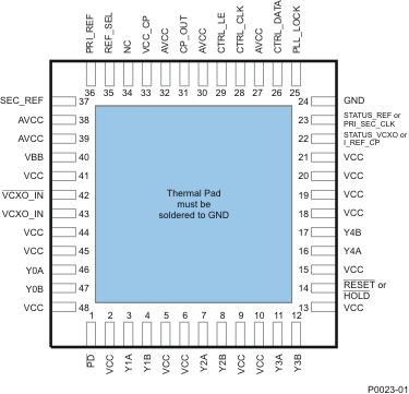
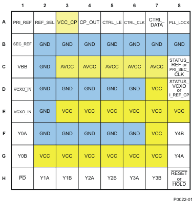
| AVCC |
C3, C4, C5, C6, C7 |
27, 30,
32, 38,
39 |
Analog Power |
3.3-V analog power supply. There is no internal connection between AVCC and VCC. It is recommended that AVCC use its own supply filter. |
| CP_OUT |
A4 |
31 |
O |
Charge pump output |
| CTRL_CLK |
A6 |
28 |
I |
LVCMOS input, serial control clock input for SPI, with hysteresis. Unused or floating inputs must be tied to proper logic level. A 20kΩ or larger pull−up resistor to VCC is recommended. |
| CTRL_DATA |
A7 |
26 |
I |
LVCMOS input, serial control data input for SPI, with hysteresis. Unused or floating inputs must be tied to proper logic level. A 20kΩ or larger pull−up resistor to VCC is recommended. |
| CTRL_LE |
A5 |
29 |
I |
LVCMOS input, control latch enable for serial programmable Interface (SPI), with hysteresis. Unused or floating inputs must be tied to proper logic level. A 20kΩ or larger pull−up resistor to VCC is recommended. |
| GND |
B2, B3, B4, B5, B6, B7, B8, C2, D2, D3, D4, D5, D6, E2, F2, F3, F4, F5, F6 |
Thermal pad and pin 24 |
Ground |
Ground |
| HOLD |
H8 |
14 |
I |
This LVCMOS input can be programmed (SPI) to act as HOLD or RESET. RESET is the default function. This pin is low active and can be activated external or via the corresponding bit in the SPI register. In case of RESET, the charge pump (CP) is switched to 3-state and all counters (N, M, P) are reset to zero (the initial divider settings are maintained in SPI registers). The LVPECL outputs are static low and high respectively and the LVCMOS outputs are all low or high if inverted. RESET is not edge triggered and should have a pulse duration of at least 5 ns. |
| In case of HOLD, the CP is switched in to 3-state mode only. After HOLD is released and with the next valid reference clock cycle the charge pump is switched back in to normal operation (CP stays in 3-state as long as no reference clock is valid). During HOLD, the P divider and all outputs Yx are at normal operation. This mode allows an external control of the frequency hold-over mode. |
| The input has an internal 150-kΩ pullup resistor. |
| I_REF_CP |
D8 |
22 |
O |
This LVCMOS output can be programmed (SPI) to provide either the STATUS_VCXO information or serve as current path for the charge pump (CP). STATUS_VCXO is the default setting. |
| In case of STATUS_VCXO, the LVCMOS output provides the status of the VCXO input (frequencies above 2 MHz are interpreted as valid clock; active high). |
| In case of I_REF_CP, it provides the current path for the external reference resistor (12 kΩ ±1%) to support an accurate charge pump current, optional. Do not use any capacitor across this resistor to prevent noise coupling via this node. If the internal 12 kΩ is selected (default setting), this pin can be left open. |
| PD |
H1 |
1 |
I |
LVCMOS input, asynchronous power down (PD) signal. This pin is low active and can be activated external or by the corresponding bit in the SPI register (in case of logic high, the SPI setting is valid). Switches the device into power-down mode. Resets M- and N-Divider, 3-states charge pump, STATUS_REF, or PRI_SEC_CLK pin, STATUS_VCXO or I_REF_CP pin, PLL_LOCK pin, VBB pin and all Yx outputs. Sets the SPI register to default value; has internal 150-kΩ pullup resistor. It is recommended to ramp up the PD with the same time as VCC and AVCC or later. The ramp up rate of the PD should not be faster than the ramp up rate of VCC and AVCC. |
| PLL_LOCK |
A8 |
25 |
I/O |
LVCMOS output for PLL_LOCK information. This pin is set high if the PLL is in lock (see feature description). This output can be programmed to be digital lock detect or analog lock detect (see feature description). |
| The PLL is locked (set high), if the rising edge either of PRI_REF or SEC_REF clock and VCXO_IN clock at the phase frequency detector (PFD) are inside the lock detect window for a predetermined number of successive clock cycles. |
| The PLL is out-of-lock (set low), if the rising edge of either the PRI_REF or SEC_REF) clock and VCXO_IN clock at the PFD are outside the lock detect window or if a certain frequency offset between reference frequency and feedback frequency (VCXO) is detected. |
| Both, the lock detect window and the number of successive clock cycles are user definable (via SPI). |
| PRI_REF |
A1 |
36 |
I |
LVCMOS input for the primary reference clock, with an internal 150-kΩ pullup resistor and input hysteresis. |
| REF_SEL |
A2 |
35 |
I |
LVCMOS reference clock selection input. In the manual mode the REF_SEL signal selects one of the two input clocks:
REF_SEL [1]: PRI_REF is selected;
REF_SEL [0]: SEC_REF is selected;
The input has an internal 150-kΩ pullup resistor. |
| RESET |
H8 |
14 |
I |
This LVCMOS input can be programmed (SPI) to act as HOLD or RESET. RESET is the default function. This pin is low active and can be activated external or via the corresponding bit in the SPI register. In case of RESET, the charge pump (CP) is switched to 3-state and all counters (N, M, P) are reset to zero (the initial divider settings are maintained in SPI registers). The LVPECL outputs are static low and high respectively and the LVCMOS outputs are all low or high if inverted. RESET is not edge triggered and should have a pulse duration of at least 5 ns. |
| In case of HOLD, the CP is switched in to 3-state mode only. After HOLD is released and with the next valid reference clock cycle the charge pump is switched back in to normal operation (CP stays in 3-state as long as no reference clock is valid). During HOLD, the P divider and all outputs Yx are at normal operation. This mode allows an external control of the frequency hold-over mode. |
| The input has an internal 150-kΩ pullup resistor. |
| SEC_REF |
B1 |
37 |
I |
LVCMOS input for the secondary reference clock, with an internal 150-kΩ pullup resistor and input hysteresis. |
| STATUS_REF or PRI_SEC_CLK |
C8 |
23 |
O |
This output can be programmed (SPI) to provide either the STATUS_REF or PRI_SEC_CLK information. This pin is set high if one of the STATUS conditions is valid. STATUS_REF is the default setting. |
| In case of STATUS_REF, the LVCMOS output provides the Status of the Reference Clock. If a reference clock with a frequency above 2 MHz is provided to PRI_REF or SEC_REF STATUS_REF will be set high. |
| In case of PRI_SEC_CLK, the LVCMOS output indicates whether the primary clock [high] or the secondary clock [low] is selected. |
| STATUS_VCXO |
D8 |
22 |
O |
This LVCMOS output can be programmed (SPI) to provide either the STATUS_VCXO information or serve as current path for the charge pump (CP). STATUS_VCXO is the default setting. |
| In case of STATUS_VCXO, the LVCMOS output provides the status of the VCXO input (frequencies above 2 MHz are interpreted as valid clock; active high). |
| In case of I_REF_CP, it provides the current path for the external reference resistor (12 kΩ ±1%) to support an accurate charge pump current, optional. Do not use any capacitor across this resistor to prevent noise coupling via this node. If the internal 12 kΩ is selected (default setting), this pin can be left open. |
| VBB |
C1 |
40 |
O |
Bias voltage output to be used to bias unused complementary input VCXO_IN for single ended signals. The output of VBB is VCC – 1.3 V. The output current is limited to about 1.5 mA. |
| VCC |
D7, E3,
E4, E5,
E6, E7,
E8, F7,
G2, G3,
G4, G5,
G6, G7 |
2, 5, 6,
9, 10,
13, 15,
18, 19,
20, 21,
41, 44,
45; 48 |
Power |
3.3-V supply. VCC and AVCC should always have the same supply voltage. It is recommended that AVCC use its own supply filter. |
| VCC_CP |
A3 |
33 |
Power |
This is the charge pump power supply pin used to have the same supply as the external VCO. It can be set from 2.3 V to 3.6 V. |
| VCXO_IN |
E1 |
43 |
I |
VCXO LVPECL input |
| VCXO_IN |
D1 |
42 |
I |
Complementary VCXO LVPECL input |
Y0A:Y0B
Y1A:Y1B
Y2A:Y2B
Y3A:Y3B
Y4A:Y4B |
F1, G1,
H2, H3,
H4, H5,
H6, H7,
G8, F8 |
46, 47,
3, 4,
7, 8,
11,12,
16, 17 |
O |
The outputs of the CDCM7005 are user definable and can be any combination of up to five LVPECL outputs or up to 10 LVCMOS outputs. The outputs are selectable via SPI (Word 1, Bit 2-6). The power-up setting is all outputs are LVPECL. |

