ZHCS416F August 2011 – October 2014 CC1175
PRODUCTION DATA.
- 1 器件概述
- 2修订历史记录
- 3Terminal Configuration and Functions
-
4Specifications
- 4.1 Absolute Maximum Ratings
- 4.2 Handling Ratings
- 4.3 Recommended Operating Conditions (General Characteristics)
- 4.4 Thermal Resistance Characteristics for RHB Package
- 4.5 RF Characteristics
- 4.6 Regulatory Standards
- 4.7 Current Consumption, Static Modes
- 4.8 Current Consumption, Transmit Modes
- 4.9 Transmit Parameters
- 4.10 PLL Parameters
- 4.11 Wake-up and Timing
- 4.12 High-Speed Crystal Oscillator
- 4.13 High-Speed Clock Input (TCXO)data to TCXO table
- 4.14 32-kHz Clock Input
- 4.15 Low-Speed RC Oscillator
- 4.16 I/O and Reset
- 4.17 Temperature Sensor
- 4.18 Typical Characteristics
- 5Detailed Description
- 6Typical Application Circuit
- 7器件和文档支持
- 8机械封装和可订购信息
4 Specifications
All measurements performed on CC1120EM_868_915 rev.1.0.1, CC1120EM_955 rev.1.2.1, CC1120EM_420_470 rev.1.0.1, or CC1120EM_169 rev.1.2.
4.1 Absolute Maximum Ratings(1)(2)
| PARAMETER | MIN | MAX | UNIT | CONDITION |
|---|---|---|---|---|
| Supply voltage (VDD, AVDD_x) | –0.3 | 3.9 | V | All supply pins must have the same voltage |
| Voltage on any digital pin | –0.3 | VDD+0.3 | V | max 3.9 |
| Voltage on analog pins (including DCPL pins) |
–0.3 | 2.0 | V |
4.2 Handling Ratings
| MIN | MAX | UNIT | ||||
|---|---|---|---|---|---|---|
| Tstg | Storage temperature range | –40 | 125 | °C | ||
| VESD | Electrostatic discharge (ESD) performance: | Human body model (HBM), per ANSI/ESDA/JEDEC JS001(1) | –2 | 2 | kV | |
| Charged device model (CDM), per JESD22-C101(2) | All pins | –500 | 500 | V | ||
4.3 Recommended Operating Conditions (General Characteristics)
| PARAMETER | MIN | TYP | MAX | UNIT | CONDITION |
|---|---|---|---|---|---|
| Voltage supply range | 2.0 | 3.6 | V | All supply pins must have the same voltage | |
| Voltage on digital inputs | 0 | VDD | V | ||
| Temperature range | –40 | 85 | °C | Ambient |
4.4 Thermal Resistance Characteristics for RHB Package
| °C/W(1) | AIR FLOW (m/s)(2) | ||
|---|---|---|---|
| RθJC | Junction-to-case (top) | 21.1 | 0.00 |
| RθJB | Junction-to-board | 5.3 | 0.00 |
| RθJA | Junction-to-free air | 31.3 | 0.00 |
| PsiJT | Junction-to-package top | 0.2 | 0.00 |
| PsiJB | Junction-to-board | 5.3 | 0.00 |
| RθJC | Junction-to-case (bottom) | 0.8 | 0.00 |
- JESD51-2, Integrated Circuits Thermal Test Method Environmental Conditions - Natural Convection (Still Air)
- JESD51-3, Low Effective Thermal Conductivity Test Board for Leaded Surface Mount Packages
- JESD51-7, High Effective Thermal Conductivity Test Board for Leaded Surface Mount Packages
- JESD51-9, Test Boards for Area Array Surface Mount Package Thermal Measurements
4.5 RF Characteristics
| PARAMETER | MIN | TYP | MAX | UNIT | CONDITION |
|---|---|---|---|---|---|
| Frequency bands | 820 | 960 | MHz | ||
| 410 | 480 | MHz | |||
| (273.3) | (320) | MHz | For more information, see SWRA398, Using the CC112x/CC1175 at 274 to 320 MHz. | ||
| 164 | 192 | MHz | |||
| (205) | (240) | MHz | Contact TI for more information about the use of these frequency bands. | ||
| (136.7) | (160) | MHz | |||
| Frequency resolution | 30 | Hz | In 820– to 960–MHz band | ||
| 15 | Hz | In 410– to 480–MHz band | |||
| 6 | Hz | In 164– to 192–MHz band | |||
| Data rate | 0 | 200 | kbps | Packet mode | |
| 0 | 100 | kbps | Transparent mode | ||
| Data rate step size | 1e-4 | bps |
4.6 Regulatory Standards
| PERFORMANCE MODE | FREQUENCY BAND | SUITABLE FOR COMPLIANCE WITH | COMMENTS |
|---|---|---|---|
| High-performance mode | 820–960 MHz | ARIB T-108 | Performance also suitable for systems targeting maximum allowed output power in the respective bands, using a range extender such as the CC1190 device |
| ARIB T-96 | |||
| ETSI EN 300 220 | |||
| ETSI EN 54-25 | |||
| FCC Part 101 | |||
| FCC Part 24 Submask D | |||
| FCC Part 15.247 | |||
| FCC Part 15.249 | |||
| FCC Part 90 Mask G | |||
| FCC Part 90 Mask J | |||
| 410–480 MHz | ARIB T-67 | Performance also suitable for systems targeting maximum allowed output power in the respective bands, using a range extender | |
| ARIB RCR STD-30 | |||
| ETSI EN 300 220 | |||
| FCC Part 90 Mask D | |||
| FCC Part 90 Mask G | |||
| 164–192 MHz | ETSI EN 300 220 | Performance also suitable for systems targeting maximum allowed output power in the respective bands, using a range extender | |
| FCC Part 90 Mask D | |||
| Low-power mode | 820–960 MHz | ETSI EN 300 220 | |
| FCC Part 15.247 | |||
| FCC Part 15.249 | |||
| 410–480 MHz | ETSI EN 300 220 | ||
| 164–192 MHz | ETSI EN 300 220 |
4.7 Current Consumption, Static Modes
TA = 25°C, VDD = 3.0 V if nothing else is stated| PARAMETER | MIN | TYP | MAX | UNIT | CONDITION |
|---|---|---|---|---|---|
| Power down with retention | 0.12 | 1 | µA | ||
| 0.5 | µA | Low-power RC oscillator running | |||
| XOFF mode | 170 | µA | Crystal oscillator / TCXO disabled | ||
| IDLE mode | 1.3 | mA | Clock running, system waiting with no radio activity |
4.8 Current Consumption, Transmit Modes
4.8.1 950-MHz Band (High-Performance Mode)
TA = 25°C, VDD = 3.0 V if nothing else is stated
| PARAMETER | MIN | TYP | MAX | UNIT | CONDITION |
|---|---|---|---|---|---|
| TX current consumption +10 dBm | 37 | mA | |||
| TX current consumption 0 dBm | 26 | mA |
4.8.2 868-, 915-, and 920-MHz Bands (High-Performance Mode)
TA = 25°C, VDD = 3.0 V if nothing else is stated
| PARAMETER | MIN | TYP | MAX | UNIT | CONDITION |
|---|---|---|---|---|---|
| TX current consumption +14 dBm | 45 | mA | |||
| TX current consumption +10 dBm | 34 | mA |
4.8.3 434-MHz Band (High-Performance Mode)
TA = 25°C, VDD = 3.0 V if nothing else is stated
| PARAMETER | MIN | TYP | MAX | UNIT | CONDITION |
|---|---|---|---|---|---|
| TX current consumption +15 dBm | 50 | mA | |||
| TX current consumption +14 dBm | 45 | mA | |||
| TX current consumption +10 dBm | 34 | mA |
4.8.4 169-MHz Band (High-Performance Mode)
TA = 25°C, VDD = 3.0 V if nothing else is stated
| PARAMETER | MIN | TYP | MAX | UNIT | CONDITION |
|---|---|---|---|---|---|
| TX current consumption +15 dBm | 54 | mA | |||
| TX current consumption +14 dBm | 49 | mA | |||
| TX current consumption +10 dBm | 41 | mA |
4.8.5 Low-Power Mode
TA = 25°C, VDD = 3.0 V, fc = 869.5 MHz if nothing else is stated
| PARAMETER | MIN | TYP | MAX | UNIT | CONDITION |
|---|---|---|---|---|---|
| TX current consumption +10 dBm | 32 | mA |
4.9 Transmit Parameters
TA = 25°C, VDD = 3.0 V, fc = 869.5 MHz if nothing else is stated
| PARAMETER | MIN | TYP | MAX | UNIT | CONDITION |
|---|---|---|---|---|---|
| Max output power | +12 | dBm | At 950 MHz | ||
| +14 | dBm | At 915 and 920 MHz | |||
| +15 | dBm | At 915 and 920 MHz with VDD = 3.6 V | |||
| +15 | dBm | At 868 MHz | |||
| +16 | dBm | At 868 MHz with VDD = 3.6 V | |||
| +15 | dBm | At 433 MHz | |||
| +16 | dBm | At 433 MHz with VDD = 3.6 V | |||
| +15 | dBm | At 169 MHz | |||
| +16 | dBm | At 169 MHz with VDD = 3.6 V | |||
| Min output power | –11 | dBm | Within fine step size range | ||
| –40 | dBm | Within coarse step size range | |||
| Output power step size | 0.4 | dB | Within fine step size range | ||
| Adjacent channel power | –75 | dBc | 4-GFSK 9.6 kbps in 12.5-kHz channel, measured in 100-Hz bandwidth at 434 MHz (FCC Part 90 Mask D compliant) | ||
| –58 | dBc | 4-GFSK 9.6 kbps in 12.5-kHz channel, measured in 8.75-kHz bandwidth (ETSI–300 220 compliant) | |||
| –61 | dBc | 2-GFSK 2.4 kbps in 12.5-kHz channel, 1.2-kHz deviation | |||
| Spurious emissions (Not including harmonics) |
<–60 | dBm | |||
| Harmonics | Transmission at +14 dBm (or maximum allowed in applicable band where this is less than +14 dBm) using TI reference design Emissions measured according to ARIB T-96 in 950-MHz band, ETSI EN 300 220 in 169-, 433-, and 868-MHz bands and FCC Part 15.247 in 450- and 915-MHz band Fourth harmonic in 915-MHz band will require extra filtering to meet FCC requirements if transmitting for long intervals (>50-ms periods). |
||||
| Second Harm, 169 MHz | –39 | dBm | |||
| Third Harm, 169 MHz | –58 | dBm | |||
| Second Harm, 433 MHz | –56 | dBm | |||
| Third Harm, 433 MHz | –51 | dBm | |||
| Second Harm, 450 MHz | –60 | dBm | |||
| Third Harm, 450 MHz | –45 | dBm | |||
| Second Harm, 868 MHz | –40 | dBm | |||
| Third Harm, 868 MHz | –42 | dBm | |||
| Second Harm, 915 MHz | 56 | dBuV/m | |||
| Third Harm, 915 MHz | 52 | dBuV/m | |||
| Fourth Harm, 915 MHz | 60 | dBuV/m | |||
| Second Harm, 950 MHz | –58 | dBm | |||
| Third Harm, 950 MHz | –42 | dBm | |||
| Optimum load impedance | |||||
| 868-, 915-, and 920-MHz bands | 35 + j35 | Ω | |||
| 433-MHz band | 55 + j25 | Ω | |||
| 169-MHz band | 80 + j0 | Ω | |||
4.10 PLL Parameters
4.10.1 High-Performance Mode
TA = 25°C, VDD = 3.0 V, fc = 869.5 MHz if nothing else is stated
| PARAMETER | MIN | TYP | MAX | UNIT | CONDITION |
|---|---|---|---|---|---|
| Phase noise in 950-MHz band | –99 | dBc/Hz | ± 10 kHz offset | ||
| –99 | dBc/Hz | ± 100 kHz offset | |||
| –123 | dBc/Hz | ± 1 MHz offset | |||
| Phase noise in 868-, 915-, and 920-MHz bands | –99 | dBc/Hz | ± 10 kHz offset | ||
| –100 | dBc/Hz | ± 100 kHz offset | |||
| –122 | dBc/Hz | ± 1 MHz offset | |||
| Phase noise in 433-MHz band | –106 | dBc/Hz | ± 10 kHz offset | ||
| –107 | dBc/Hz | ± 100 kHz offset | |||
| –127 | dBc/Hz | ± 1 MHz offset | |||
| Phase noise in 169-MHz band | –111 | dBc/Hz | ± 10 kHz offset | ||
| –116 | dBc/Hz | ± 100 kHz offset | |||
| –135 | dBc/Hz | ± 1 MHz offset |
4.10.2 Low-Power Mode
TA = 25°C, VDD = 3.0 V, fc = 869.5 MHz if nothing else is stated
| PARAMETER | MIN | TYP | MAX | UNIT | CONDITION |
|---|---|---|---|---|---|
| Phase noise in 950-MHz band | –90 | dBc/Hz | ± 10 kHz offset | ||
| –92 | dBc/Hz | ± 100 kHz offset | |||
| –124 | dBc/Hz | ± 1 MHz offset | |||
| Phase noise in 868- and 915-MHz bands | –95 | dBc/Hz | ± 10 kHz offset | ||
| –95 | dBc/Hz | ± 100 kHz offset | |||
| –124 | dBc/Hz | ± 1 MHz offset | |||
| Phase noise in 433-MHz band | –98 | dBc/Hz | ± 10 kHz offset | ||
| –102 | dBc/Hz | ± 100 kHz offset | |||
| –129 | dBc/Hz | ± 1 MHz offset | |||
| Phase noise in 169-MHz band | –106 | dBc/Hz | ± 10 kHz offset | ||
| –110 | dBc/Hz | ± 100 kHz offset | |||
| –136 | dBc/Hz | ± 1 MHz offset |
4.11 Wake-up and Timing
TA = 25°C, VDD = 3.0 V, fc = 869.5 MHz if nothing else is stated
| PARAMETER | MIN | TYP | MAX | UNIT | CONDITION |
|---|---|---|---|---|---|
| Powerdown to IDLE | 0.4 | ms | Depends on crystal | ||
| IDLE to TX | 166 | µs | Calibration disabled | ||
| 461 | µs | Calibration enabled | |||
| TX to IDLE time | 296 | µs | Calibrate when leaving TX enabled | ||
| 0 | µs | Calibrate when leaving TX disabled | |||
| Frequency synthesizer calibration | 391 | µs | When using SCAL strobe |
4.12 High-Speed Crystal Oscillator
TA = 25°C, VDD = 3.0 V if nothing else is stated
| PARAMETER | MIN | TYP | MAX | UNIT | CONDITION |
|---|---|---|---|---|---|
| Crystal frequency | 32 | 44 | MHz | It is expected that there will be an increase in spurious emissions when the RF channel is close to multiples of XOSC in TX. We recommend that the level of spurious emissions be evaluated if the RF channel is closer than 1 MHz to multiples of XOSC in TX. | |
| Load capacitance (CL) | 10 | pF | |||
| ESR | 60 | Ω | Simulated over operating conditions | ||
| Start-up time | 0.4 | ms | Depends on crystal |
4.13 High-Speed Clock Input (TCXO)
TA = 25°C, VDD = 3.0 V if nothing else is stated
| PARAMETER | MIN | TYP | MAX | UNIT | CONDITION |
|---|---|---|---|---|---|
| Clock frequency | 32 | 44 | MHz | ||
| TCXO with CMOS output | TCXO with CMOS output directly coupled to pin EXT_OSC | ||||
| High input voltage | 1.4 | VDD | V | ||
| Low input voltage | 0 | 0.6 | V | ||
| Rise / Fall time | 2 | ns | |||
| Clipped sine output | TCXO clipped sine output connected to pin EXT_OSC through series capacitor | ||||
| Clock input amplitude (peak-to-peak) | 0.8 | 1.5 | V |
4.14 32-kHz Clock Input
TA = 25°C, VDD = 3.0 V if nothing else is stated
| PARAMETER | MIN | TYP | MAX | UNIT | CONDITION |
|---|---|---|---|---|---|
| Clock frequency | 32 | kHz | |||
| 32 kHz clock input pin input high voltage | 0.8×VDD | V | |||
| 32 kHz clock input pin input low voltage | 0.2×VDD | V |
4.15 Low-Speed RC Oscillator
TA = 25°C, VDD = 3.0 V if nothing else is stated
| PARAMETER | MIN | TYP | MAX | UNIT | CONDITION |
|---|---|---|---|---|---|
| Frequency | 32/40 | kHz | After calibration (calibrated against the high-speed XOSC) | ||
| Frequency accuracy after calibration | ±0.1 | % | Relative to frequency reference (for example, 32-MHz crystal or TCXO) | ||
| Initial calibration time | 1.6 | ms |
4.16 I/O and Reset
TA = 25°C, VDD = 3.0 V if nothing else is stated
| PARAMETER | MIN | TYP | MAX | UNIT | CONDITION |
|---|---|---|---|---|---|
| Logic input high voltage | 0.8×VDD | V | |||
| Logic input low voltage | 0.2×VDD | V | |||
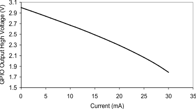
| Logic output high voltage | 0.8×VDD | V | At 4-mA output load or less | ||
| Logic output low voltage | 0.2×VDD | V | |||
| Power-on reset threshold | 1.3 | V | Voltage on DVDD pin |
4.17 Temperature Sensor
TA = 25°C, VDD = 3.0 V if nothing else is stated
| PARAMETER | MIN | TYP | MAX | UNIT | CONDITION |
|---|---|---|---|---|---|
| Temperature sensor range | –40 | 85 | °C | ||
| Temperature coefficient | 2.66 | mV / °C | Change in sensor output voltage versus change in temperature | ||
| Typical output voltage | 794 | mV | Typical sensor output voltage at TA = 25°C, VDD = 3.0 V |
||
| VDD coefficient | 1.17 | mV / V | Change in sensor output voltage versus change in VDD |
The CC1175 device can be configured to provide a voltage proportional to temperature on GPIO1. The temperature can be estimated by measuring this voltage (see Section 4.17). For more information, see the temperature sensor design note (SWRA415).
4.18 Typical Characteristics
TA = 25°C, VDD = 3.0 V, fc = 869.5 MHz if nothing else is stated.
All measurements performed on CC1120EM_868_915 rev.1.0.1, CC1120EM_955 rev.1.2.1, CC1120EM_420_470 rev.1.0.1 or CC1120EM_169 rev.1.2 (fxosc = 32 MHz), and CC1125EM_868_915 rev.1.1.0, CC1125EM_420_470 rev.1.1.0, CC1125EM_169 rev.1.1.0, CC1125EM-Cat1-868 (fxosc = 40 MHz).
Figure 4-6 was measured at the 50-Ω antenna connector.
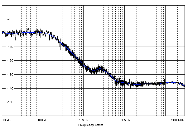 Figure 4-1 Phase Noise in 868-MHz Band
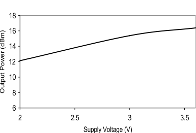 Figure 4-3 Output Power vs Voltage
Max Setting, 170 MHz
vs PA Power Setting
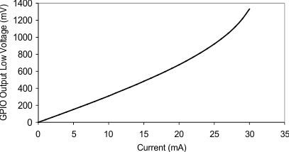
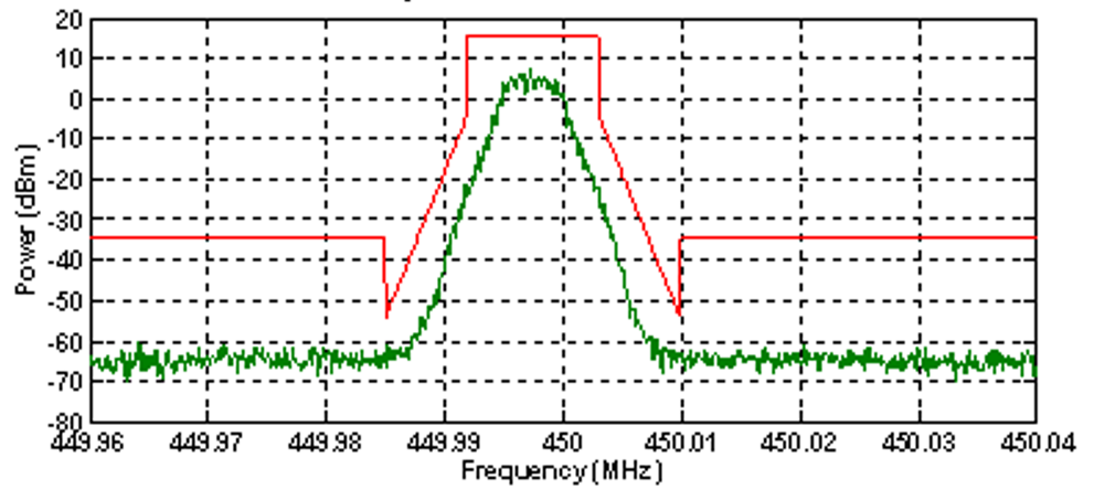
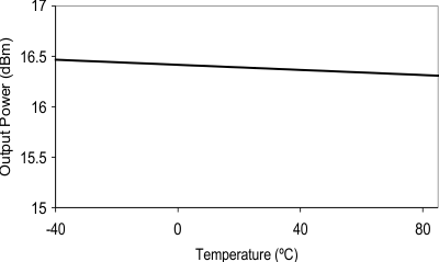 Figure 4-2 Output Power vs Temperature
Max Setting, 170 MHz, 3.6 V
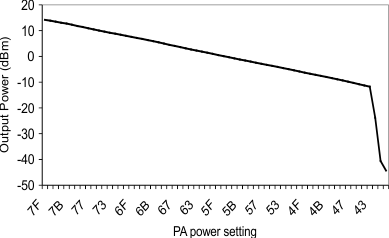 Figure 4-4 Output Power
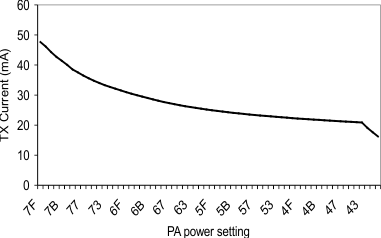
 vs PA Power Setting
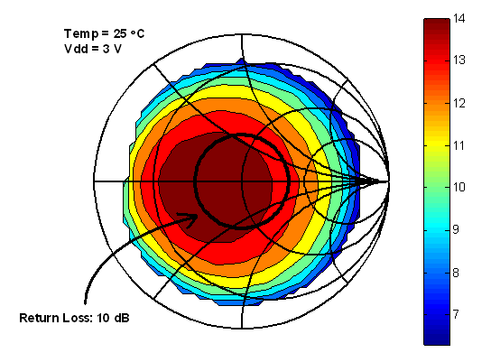 Figure 4-6 Output Power vs Load Impedance (+14-dBm Setting)