ZHCSAN2E december   2012  – april 2021 BQ7716

PRODUCTION DATA  

  1.   1
  2. 特性
  3. 应用
  4. 说明
  5. Revision History
  6. Device Comparison Table
  7. Pin Configuration and Functions
  8. Specifications
    1. 7.1 Absolute Maximum Ratings
    2. 7.2 ESD Ratings
    3. 7.3 Recommended Operating Conditions
    4. 7.4 Thermal Information
    5. 7.5 Electrical Characteristics
    6. 7.6 Typical Characteristics
  9. Detailed Description
    1. 8.1 Overview
    2. 8.2 Functional Block Diagram
    3. 8.3 Feature Description
      1. 8.3.1 Sense Positive Input for Vx
      2. 8.3.2 Output Drive, OUT
      3. 8.3.3 Supply Input, VDD
      4. 8.3.4 External Delay Capacitor, CD
    4. 8.4 Device Functional Modes
      1. 8.4.1 NORMAL Mode
      2. 8.4.2 OVERVOLTAGE Mode
      3. 8.4.3 Customer Test Mode
  10. Application and Implementation
    1. 9.1 Application Information
    2. 9.2 Typical Application
      1. 9.2.1 Design Requirements
      2. 9.2.2 Detailed Design Procedure
      3. 9.2.3 Application Curves
  11. 10Power Supply Recommendations
  12. 11Layout
    1. 11.1 Layout Guidelines
    2. 11.2 Layout Example
  13. 12Device and Documentation Support
    1. 12.1 Receiving Notification of Documentation Updates
    2. 12.2 支持资源
    3. 12.3 Trademarks
    4. 12.4 静电放电警告
    5. 12.5 Export Control Notice
    6. 12.6 术语表
  14. 13Mechanical, Packaging, and Orderable Information

封装选项

机械数据 (封装 | 引脚)
散热焊盘机械数据 (封装 | 引脚)
订购信息

Typical Application

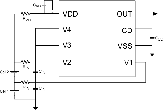
GUID-0F65D07B-4A16-44B9-B7A5-2D7F665213AA-low.gifFigure 9-2 2-Series Cell Configuration with Capacitor-Programmed Delay
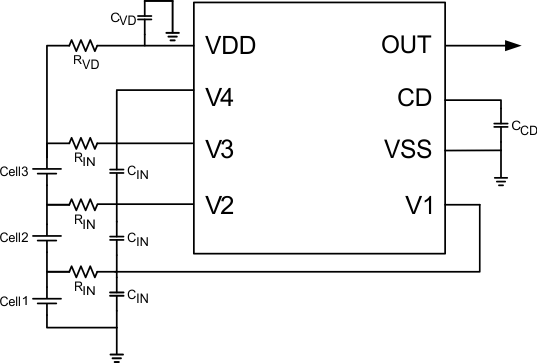
GUID-6994CC44-4591-4EBF-ACA1-57C0183AEDDB-low.gifFigure 9-3 3-Series Cell Configuration with Capacitor-Programmed Delay
Note:

In these application examples of 2 s and 3 s, an external pull-up resistor is required on the OUT terminal to configure for an Open Drain Active Low operation.