ZHCSEJ8B January 2011 – December 2015
PRODUCTION DATA.
- 1 特性
- 2 应用
- 3 说明
- 4 修订历史记录
- 5 说明 (续)
- 6 Pin Configuration and Functions
-
7 Specifications
- 7.1 Absolute Maximum Ratings
- 7.2 ESD Ratings
- 7.3 Recommended Operating Conditions
- 7.4 Thermal Information
- 7.5 Electrical Characteristics: General Purpose I/O
- 7.6 Supply Current
- 7.7 REG27 LDO
- 7.8 Coulomb Counter
- 7.9 ADC
- 7.10 External Capacitor Voltage Balance Drive
- 7.11 Capacitor Voltage Monitor
- 7.12 Internal Temperature Sensor
- 7.13 Thermistor Measurement Support
- 7.14 Internal Thermal Shutdown
- 7.15 High-Frequency Oscillator
- 7.16 Low-Frequency Oscillator
- 7.17 RAM Backup
- 7.18 Flash
- 7.19 Current Protection Thresholds
- 7.20 Current Protection Timing
- 7.21 Timing Requirements: SMBus
- 7.22 Typical Characteristics
-
8 Detailed Description
- 8.1 Overview
- 8.2 Functional Block Diagram
- 8.3
Feature Description
- 8.3.1 Capacitance Monitoring and Learning
- 8.3.2 Capacitor Voltage Balancing
- 8.3.3 Charge Control
- 8.3.4 Lifetime Data Gathering
- 8.3.5
Safety Detection Features
- 8.3.5.1 Capacitor Overvoltage (OV)
- 8.3.5.2 Capacitor Voltage Imbalance (CIM)
- 8.3.5.3 Weak Capacitor (CLBAD)
- 8.3.5.4 Overtemperature (OT)
- 8.3.5.5 Overcurrent During Charging (OC Chg)
- 8.3.5.6 Overcurrent During Discharging (OC Dsg)
- 8.3.5.7 Short-Circuit During Charging (SC Chg)
- 8.3.5.8 Short-Circuit During Discharging (SC Dsg)
- 8.3.5.9 AFE Watchdog (WDF)
- 8.3.5.10 Integrated AFE Communication Fault (AFE_C)
- 8.3.5.11 Data Flash Fault (DFF)
- 8.3.5.12 FAULT Indication (FAULT Pin)
- 8.3.6 Communications
- 8.3.7 Security (Enables and Disables Features)
- 8.3.8
Measurement System Calibration
- 8.3.8.1 Coulomb Counter Deadband
- 8.3.8.2 Auto Calibration
- 8.3.8.3 Current Gain
- 8.3.8.4 CC Delta
- 8.3.8.5 Cap1 K-factor
- 8.3.8.6 Cap2 K-factor
- 8.3.8.7 Cap3 K-factor
- 8.3.8.8 Cap4 K-factor
- 8.3.8.9 Cap5 K-factor
- 8.3.8.10 K-factor Override Flag
- 8.3.8.11 System Voltage K-factor
- 8.3.8.12 Stack Voltage K-factor
- 8.3.8.13 K-factor Stack Override Flag
- 8.3.8.14 CC Offset
- 8.3.8.15 Board Offset
- 8.3.8.16 Int Temp Offset
- 8.3.8.17 Ext1 Temp Offset
- 8.3.8.18 CC Current
- 8.3.8.19 Voltage Signal
- 8.3.8.20 Temp Signal
- 8.3.8.21 CC Offset Time
- 8.3.8.22 ADC Offset Time
- 8.3.8.23 Current Gain Time
- 8.3.8.24 Voltage Time
- 8.3.8.25 Temperature Time
- 8.3.8.26 Cal Mode Timeout
- 8.3.8.27 Ext Coef a1..a5, b1..b4, Ext rc0, Ext adc0
- 8.3.8.28 Rpad
- 8.3.8.29 Rint
- 8.3.8.30 Int Coef 1..4, Int Min AD, Int Max Temp
- 8.3.8.31 Filter
- 8.3.8.32 Deadband
- 8.3.8.33 CC Deadband
- 8.4 Device Functional Modes
- 8.5
Programming
- 8.5.1 Communications
- 8.5.2
SBS Commands
- 8.5.2.1 SBS Command Summary
- 8.5.2.2
SBS Command Details
- 8.5.2.2.1
ManufacturerAccess (0x00)
- 8.5.2.2.1.1 Device Type (0x0001)
- 8.5.2.2.1.2 Firmware Version (0x0002)
- 8.5.2.2.1.3 Hardware Version (0x0003)
- 8.5.2.2.1.4 DF Checksum (0x0004)
- 8.5.2.2.1.5 Seal Device (0x0020)
- 8.5.2.2.1.6 Lifetime and Capacitor Balancing Enable (0x0021)
- 8.5.2.2.1.7 FAULT Activation (0x0030)
- 8.5.2.2.1.8 FAULT Clear (0x0031)
- 8.5.2.2.1.9 CHGLVL0 Activation (0x0032)
- 8.5.2.2.1.10 CHGLVL0 Clear (0x0033)
- 8.5.2.2.1.11 CHGLVL1 Activation (0x0033)
- 8.5.2.2.1.12 CHGLVL1 Clear (0x0034)
- 8.5.2.2.1.13 Learn Load Activation (0x0037)
- 8.5.2.2.1.14 Learn Load Clear (0x0038)
- 8.5.2.2.1.15 Calibration Mode (0x0040)
- 8.5.2.2.1.16 Reset (0x0041)
- 8.5.2.2.1.17 Unseal Device (UnsealKey)
- 8.5.2.2.1.18 Extended SBS Commands
- 8.5.2.2.2 Temperature (0x08)
- 8.5.2.2.3 Voltage (0x09)
- 8.5.2.2.4 Current (0x0a)
- 8.5.2.2.5 ESR (0x0b)
- 8.5.2.2.6 RelativeStateofCharge (0x0d)
- 8.5.2.2.7 Health (0x0e)
- 8.5.2.2.8 Capacitance (0x10)
- 8.5.2.2.9 ChargingCurrent (0x14)
- 8.5.2.2.10 ChargingVoltage (0x15)
- 8.5.2.2.11 CapacitorVoltage5..1 (0x3b..0x3f)
- 8.5.2.2.12 Extended SBS Commands
- 8.5.2.2.1
ManufacturerAccess (0x00)
- 8.5.3
Data Flash
- 8.5.3.1 Accessing Data Flash
- 8.5.3.2 Data Flash Interface
- 8.5.3.3 Data Flash Summary
- 8.5.3.4
Specific Data Flash Programming Details
- 8.5.3.4.1 OC Dsg
- 8.5.3.4.2 OC Dsg Time
- 8.5.3.4.3 SC Dsg Cfg
- 8.5.3.4.4 SC Chg Cfg
- 8.5.3.4.5 Initial Full Charge Capacitance
- 8.5.3.4.6 Full Charge Capacitance
- 8.5.3.4.7 Firmware Version
- 8.5.3.4.8 Hardware Revision
- 8.5.3.4.9 Manuf. Info
- 8.5.3.4.10 Operation Cfg
- 8.5.3.4.11 FET ACTION
- 8.5.3.4.12 FAULT
- 8.5.3.4.13 AFE State_CTL
- 8.5.3.4.14 Measurement Margin %
- 8.5.3.4.15 Timer
- 8.5.3.4.16 V Chg Nominal
- 8.5.3.4.17 V Chg A
- 8.5.3.4.18 V Chg B
- 8.5.3.4.19 V Chg Max
- 8.5.3.4.20 Min Voltage
- 8.5.3.4.21 Learning Frequency
- 8.5.3.4.22 Dsg Current Threshold
- 8.5.3.4.23 Chg Current Threshold
- 8.5.3.4.24 Quit Current
- 9 Application and Implementation
- 10Power Supply Recommendations
- 11Layout
- 12器件和文档支持
- 13机械、封装和可订购信息
11 Layout
11.1 Layout Guidelines
A capacitance monitor circuit board is a challenging environment due to the fundamental incompatibility of high current traces and ultra-low current semiconductor devices. The best way to protect against unwanted trace-to-trace coupling is with a component placement, where the high-current section is on the opposite side of the board from the electronic devices. Every attempt must be made to route high-current traces away from signal traces, which enter the bq33100 directly. IC references and registers can be disturbed and in rare cases damaged due to magnetic and capacitive coupling from the high-current path.
NOTE
During surge current and ESD events, the high-current traces appear inductive and can couple unwanted noise into sensitive nodes of the gas gauge electronics.
The learning load components can become heated depending on the component values selected. TI recommends that any heat is dissipated away from the bq33100 to ensure its maxim operating temperature is not exceeded.
11.2 Layout Example
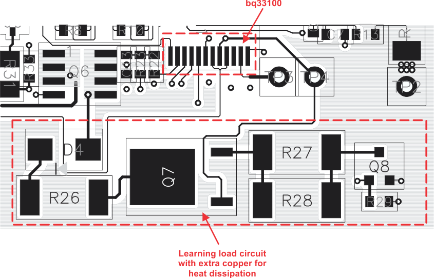 Figure 20. bq33100 Board Layout
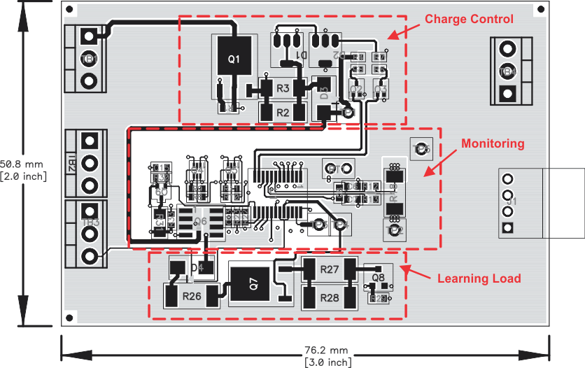 Figure 21. Top Layer
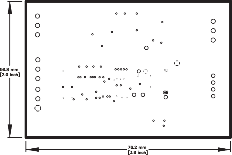 Figure 22. Internal Layer 1
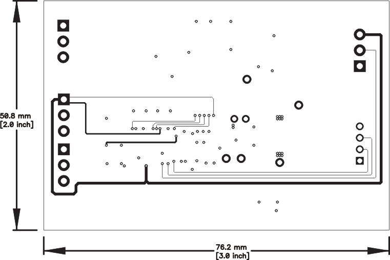 Figure 23. Internal Layer 2
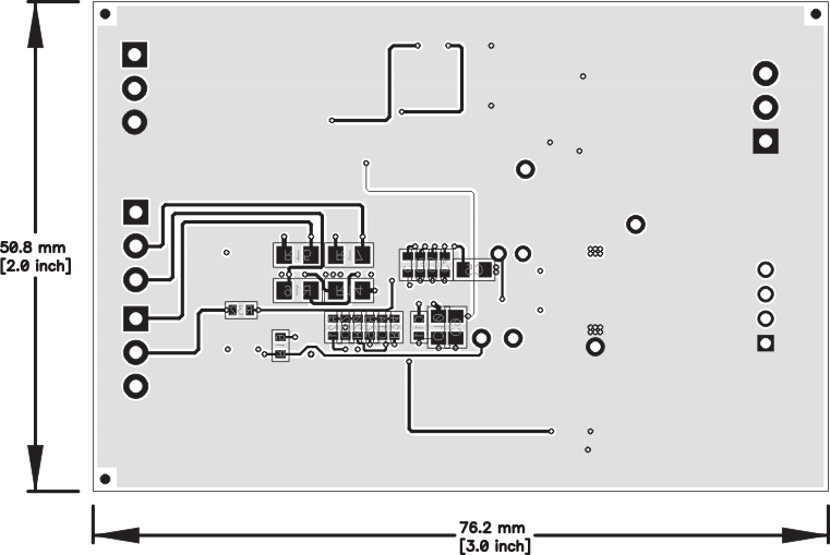 Figure 24. Bottom Layer