ZHCSE10T November   2013  – August 2022 BQ2961 , BQ2962

PRODMIX  

  1. 特性
  2. 应用
  3. 说明
  4. Revision History
  5. Device Comparison Table
  6. Pin Configuration and Functions
  7. Specifications
    1. 7.1 Absolute Maximum Ratings
    2. 7.2 ESD Ratings
    3. 7.3 Recommended Operating Conditions
    4. 7.4 Thermal Information
    5. 7.5 Electrical Characteristics
    6. 7.6 Typical Characteristics
  8. Detailed Description
    1. 8.1 Overview
    2. 8.2 Functional Block Diagram
    3. 8.3 Feature Description
      1. 8.3.1 Pin Details
        1. 8.3.1.1 Input Sense Voltage, Vx
        2. 8.3.1.2 Output Drive, OUT
        3. 8.3.1.3 Supply Input, VDD
        4. 8.3.1.4 Regulated Supply Output, REG
      2. 8.3.2 Overvoltage Sensing for OUT
      3. 8.3.3 Regulated Output Voltage and REG_EN Pin
    4. 8.4 Device Functional Modes
      1. 8.4.1 NORMAL Mode
      2. 8.4.2 OVERVOLTAGE Mode
      3. 8.4.3 UNDERVOLTAGE Mode
      4. 8.4.4 CUSTOMER TEST MODE
  9. Application and Implementation
    1. 9.1 Application Information
    2. 9.2 Typical Application
      1. 9.2.1 Design Requirements
      2. 9.2.2 Detailed Design Procedure
      3. 9.2.3 Application Curves
  10. 10Power Supply Recommendations
  11. 11Layout
    1. 11.1 Layout Guidelines
    2. 11.2 Layout Example
  12. 12Device and Documentation Support
    1. 12.1 第三方产品免责声明
    2. 12.2 Receiving Notification of Documentation Updates
    3. 12.3 支持资源
    4. 12.4 Trademarks
    5. 12.5 Electrostatic Discharge Caution
    6. 12.6 术语表
  13. 13Mechanical, Packaging, and Orderable Information

封装选项

机械数据 (封装 | 引脚)
散热焊盘机械数据 (封装 | 引脚)
订购信息

Overvoltage Sensing for OUT

In the BQ296xxx device, each cell is monitored independently. Overvoltage is detected by comparing the actual cell voltage to a protection voltage reference, VOV. If any cell voltage exceeds the programmed OV value, an internal timer circuit is activated. This timer circuit causes a factory pre-programmed fixed delay before the OUT terminal goes from inactive to active state.
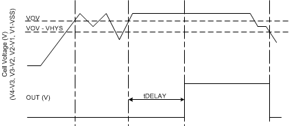
GUID-84C5CC22-BACC-4C48-B416-A2CF1FBF9765-low.gifFigure 8-1 Timing for Overvoltage Sensing for OUT