ZHCSCT0 September 2014
PRODUCTION DATA.
- 1 特性
- 2 应用
- 3 说明
- 4 简化电路原理图
- 5 修订历史记录
- 6 Pin Configuration and Functions
-
7 Specifications
- 7.1 Absolute Maximum Ratings
- 7.2 Handling Ratings
- 7.3 Recommended Operating Conditions
- 7.4 Thermal Information
- 7.5 Supply Current
- 7.6 Digital Input and Output DC Electrical Characteristics
- 7.7 Power-on Reset
- 7.8 2.5-V LDO Regulator
- 7.9 Internal Clock Oscillators
- 7.10 ADC (Temperature and Cell Measurement) Characteristics
- 7.11 Integrating ADC (Coulomb Counter) Characteristics
- 7.12 Data Flash Memory Characteristics
- 7.13 I2C-compatible Interface Communication Timing Characteristics
- 7.14 Typical Characteristics
- 8 Detailed Description
- 9 Application and Implementation
- 10Power Supply Recommendations
- 11Layout
- 12器件和文档支持
- 13机械封装和可订购信息
6 Pin Configuration and Functions
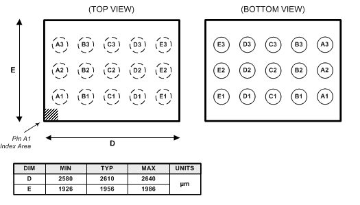
Pin Functions
| PIN | TYPE(1) | DESCRIPTION | |
|---|---|---|---|
| NAME | NUMBER | ||
| BAT | E2 | I | Cell-voltage measurement input. ADC input. TI recommends 4.8 V maximum for conversion accuracy. |
| BI/TOUT | E3 | IO | Battery-insertion detection input. Power pin for pack thermistor network. Thermistor-multiplexer control pin. Use with pullup resistor > 1 MΩ (1.8 MΩ typical). |
| BSCL | B2 | O | Battery charger clock output line for chipset communication. Use without external pullup resistor. Push-pull output. |
| BSDA | C3 | IO | Battery charger data line for chipset communication. Use without external pullup resistor. Push-pull output. |
| CE | D2 | I | Chip enable. Internal LDO is disconnected from REGIN when driven low. Note: CE has an internal ESD protection diode connected to REGIN. TI recommends maintaining VCE ≤ VREGIN under all conditions. |
| REGIN | E1 | P | Regulator input. Decouple with 0.1-μF ceramic capacitor to VSS. |
| SCL | A3 | I | Slave I2C serial communications clock input line for communication with system (master). Open-drain IO. Use with 10-kΩ pullup resistor (typical). |
| SDA | B3 | IO | Slave I2C serial communications data line for communication with system (master). Open-drain IO. Use with 10-kΩ pullup resistor (typical). |
| SOC_INT | A2 | IO | SOC state interrupts output. Generates a pulse as described in SLUUB04, bq27532-G1 Technical Reference Manual. Open-drain output. |
| SRN | B1 | AI | Analog input pin connected to the internal coulomb counter where SRN is nearest the VSS connection. Connect to 5- to 20-mΩ sense resistor. |
| SRP | A1 | AI | Analog input pin connected to the internal coulomb counter where SRP is nearest the PACK– connection. Connect to 5- to 20-mΩ sense resistor. |
| TS | D3 | AI | Pack thermistor voltage sense (use 103AT-type thermistor). ADC input. |
| VCC | D1 | P | Regulator output and bq27532-G1 device power. Decouple with 1-μF ceramic capacitor to VSS. Pin is not intended to power additional external loads. |
| VSS | C1, C2 | P | Device ground |
(1) IO = Digital input-output, AI = Analog input, P = Power connection