ZHCSB26A May 2013 – August 2014
PRODUCTION DATA.
- 1 特性
- 2 应用
- 3 说明
- 4 简化电路原理图
- 5 修订历史记录
- 6 Device Comparison Table
- 7 Pin Configuration and Functions
-
8 Specifications
- 8.1 Absolute Maximum Ratings
- 8.2 Handling Ratings
- 8.3 Recommended Operating Conditions
- 8.4 Thermal Information
- 8.5 Supply Current
- 8.6 Digital Input and Output DC Characteristics
- 8.7 LDO Regulator, Wake-up, and Auto-shutdown DC Characteristics
- 8.8 ADC (Temperature and Cell Measurement) Characteristics
- 8.9 Integrating ADC (Coulomb Counter) Characteristics
- 8.10 Integrated Sense Resistor Characteristics
- 8.11 I2C-Compatible Interface Communication Timing Characteristics
- 9 Detailed Description
- 10Application and Implementation
- 11Power Supply Recommendation
- 12Layout
- 13器件和文档支持
- 14机械封装和可订购信息
8 Specifications
8.1 Absolute Maximum Ratings
over operating free-air temperature range (unless otherwise noted)(1)| PARAMETER | MIN | MAX | UNIT | |
|---|---|---|---|---|
| VBAT | BAT pin input voltage range | –0.3 | 6 | V |
| VSRX | SRX pin input voltage range | VBAT – 0.3 | VBAT + 0.3 | V |
| VDD | VDD pin supply voltage range (LDO output) | –0.3 | 2 | V |
| VIOD | Open-drain IO pins (SDA, SCL, GPOUT) | –0.3 | 6 | V |
| VIOPP | Push-pull IO pins (BIN) | –0.3 | VDD + 0.3 | V |
| TA | Operating free-air temperature range | –40 | 85 | °C |
(1) Stresses beyond those listed under "absolute maximum ratings" may cause permanent damage to the device. These are stress ratings only, and functional operation of the device at these or any other conditions beyond those indicated under "recommended operating conditions" is not implied. Exposure to absolute-maximum-rated conditions for extended periods may affect device reliability.
8.2 Handling Ratings
| MIN | MAX | UNIT | |||
|---|---|---|---|---|---|
| Tstg | Storage temperature range | –65 | 150 | °C | |
| V(ESD) | Electrostatic discharge | Human body model (HBM), per ANSI/ESDA/JEDEC JS-001, all pins(1) | –1.5 | 1.5 | kV |
| Charged device model (CDM), per JEDEC specification JESD22-C101, all pins(2) | –250 | 250 | V | ||
(1) JEDEC document JEP155 states that 500-V HBM allows safe manufacturing with a standard ESD control process.
(2) JEDEC document JEP157 states that 250-V CDM allows safe manufacturing with a standard ESD control process.
8.3 Recommended Operating Conditions
TA = 30°C and VREGIN = VBAT = 3.6V (unless otherwise noted)| PARAMETER | TEST CONDITIONS | MIN | TYP | MAX | UNIT | |
|---|---|---|---|---|---|---|
| CBAT(1) | External input capacitor for internal LDO between BAT and VSS | Nominal capacitor values specified. Recommend a 5% ceramic X5R-type capacitor located close to the device. | 0.1 | μF | ||
| CLDO18(1) | External output capacitor for internal LDO between VDD and VSS | 0.47 | μF | |||
| VPU(1) | External pull-up voltage for open-drain pins (SDA, SCL, GPOUT) | 1.62 | 3.6 | V | ||
(1) Specified by design. Not production tested.
8.4 Thermal Information
over operating free-air temperature range (unless otherwise noted)| THERMAL METRIC(1) | bq27421-G1 | UNIT | |
|---|---|---|---|
| YZF (9 PINS) | |||
| RθJA | Junction-to-ambient thermal resistance | 107.8 | °C/W |
| RθJCtop | Junction-to-case (top) thermal resistance | 0.7 | |
| RθJB | Junction-to-board thermal resistance | 60.4 | |
| ψJT | Junction-to-top characterization parameter | 3.5 | |
| ψJB | Junction-to-board characterization parameter | 60.4 | |
| RθJCbot | Junction-to-case (bottom) thermal resistance | NA | |
(1) For more information about traditional and new thermal metrics, see the IC Package Thermal Metrics application report, SPRA953
8.5 Supply Current
TA = 30°C and VREGIN = VBAT = 3.6 V (unless otherwise noted)| PARAMETER | TEST CONDITIONS | MIN | TYP | MAX | UNIT | |
|---|---|---|---|---|---|---|
| ICC(1) | NORMAL mode current | ILOAD > Sleep Current(2) | 93 | μA | ||
| ISLP(1) | SLEEP mode current | ILOAD < Sleep Current(2) | 21 | μA | ||
| IHIB(1) | HIBERNATE mode current | ILOAD < Hibernate Current(2) | 9 | μA | ||
| ISD(1) | SHUTDOWN mode current | Fuel gauge in host commanded SHUTDOWN mode (LDO regulator output disabled) |
0.6 | μA | ||
(1) Specified by design. Not production tested.
(2) Wake Comparator Disabled.
8.6 Digital Input and Output DC Characteristics
TA = –40°C to 85°C, typical values at TA = 30°C and VREGIN = 3.6 V (unless otherwise noted)| PARAMETER | TEST CONDITIONS | MIN | TYP | MAX | UNIT | |
|---|---|---|---|---|---|---|
| VIH(OD) | Input voltage, high (2) | External pullup resistor to VPU | VPU × 0.7 | V | ||
| VIL | Input voltage, low (2)(3) | 0.6 | V | |||
| VOL | Output voltage, low (2) | 0.6 | V | |||
| IOH | Output source current, high (2)(3) | 0.5 | mA | |||
| IOL(OD) | Output sink current, low (2) | –3 | mA | |||
| CIN(1) | Input capacitance (2)(3) | 5 | pF | |||
| Ilkg | Input leakage current (SCL, SDA, BIN) |
0.1 | μA | |||
| Input leakage current (GPOUT) | 1 | |||||
(1) Specified by design. Not production tested.
(2) Open Drain pins: (SCL, SDA, GPOUT)
(3) Push-pull pin: (BIN)
8.7 LDO Regulator, Wake-up, and Auto-shutdown DC Characteristics
TA = –40°C to 85°C, typical values at TA = 30°C and VREGIN = 3.6 V (unless otherwise noted)| PARAMETER | TEST CONDITIONS | MIN | TYP | MAX | UNIT | |
|---|---|---|---|---|---|---|
| VBAT | BAT pin regulator input | 2.45 | 4.5 | V | ||
| VDD | Regulator output voltage | 1.8 | V | |||
| UVLOIT+ | VBAT undervoltage lockout LDO wake-up rising threshold |
2 | V | |||
| UVLOIT- | VBAT undervoltage lockout LDO auto-shutdown falling threshold |
1.95 | V | |||
(1) Specified by design. Not production tested.
8.8 ADC (Temperature and Cell Measurement) Characteristics
TA = –40°C to 85°C; typical values at TA = 30°C and VREGIN = 3.6 V (unless otherwise noted)| PARAMETER | TEST CONDITIONS | MIN | TYP | MAX | UNIT | |
|---|---|---|---|---|---|---|
| VIN(BAT) | BAT pin voltage measurement range. | Voltage divider enabled. | 2.45 | 4.5 | V | |
| tADC_CONV | Conversion time | 125 | ms | |||
| Effective resolution | 15 | bits | ||||
(1) Specified by design. Not tested in production.
8.9 Integrating ADC (Coulomb Counter) Characteristics
TA = –40°C to 85°C; typical values at TA = 30°C and VREGIN = 3.6 V (unless otherwise noted)| PARAMETER | TEST CONDITIONS | MIN | TYP | MAX | UNIT | |
|---|---|---|---|---|---|---|
| VSR | Input voltage range from BAT to SRX pins | BAT ± 25 | mV | |||
| tSR_CONV | Conversion time | Single conversion | 1 | s | ||
| Effective Resolution | Single conversion | 16 | bits | |||
(1) Assured by design. Not tested in production.
8.10 Integrated Sense Resistor Characteristics
TA = –40°C to 85°C; typical values at TA = 30°C and VREGIN = 3.6 V (unless otherwise noted)| PARAMETER | TEST CONDITIONS | MIN | TYP | MAX | UNIT | |
|---|---|---|---|---|---|---|
| SRXRES(2) | Resistance of Integrated Sense Resistor from SRX to VSS. | TA = 30°C | 7 | mΩ | ||
| ISRX(1) | Recommended Sense Resistor input current. | Long term RMS, average device utilization | 2000 | mA | ||
| Peak RMS current, 10% device utilization(3) | 2500 | mA | ||||
| Peak pulsed current, 250 ms maximum, 1% device utilization(3) | 3500 | mA | ||||
(1) Specified by design. Not tested in production.
(2) Firmware compensation applied for temperature coefficient of resistor.
(3) Device utilization is the long term usage profile at a specific condition compared to the average condition.
8.11 I2C-Compatible Interface Communication Timing Characteristics
TA = –40°C to 85°C; typical values at TA = 30°C and VREGIN = 3.6 V (unless otherwise noted)| PARAMETER | TEST CONDITIONS | MIN | TYP | MAX | UNIT | |
|---|---|---|---|---|---|---|
| Standard Mode (100 kHz) | ||||||
| td(STA) | Start to first falling edge of SCL | 4 | μs | |||
| tw(L) | SCL pulse duration (low) | 4.7 | μs | |||
| tw(H) | SCL pulse duration (high) | 4 | μs | |||
| tsu(STA) | Setup for repeated start | 4.7 | μs | |||
| tsu(DAT) | Data setup time | Host drives SDA | 250 | ns | ||
| th(DAT) | Data hold time | Host drives SDA | 0 | ns | ||
| tsu(STOP) | Setup time for stop | 4 | μs | |||
| t(BUF) | Bus free time between stop and start | Includes Command Waiting Time | 66 | μs | ||
| tf | SCL or SDA fall time (1) | 300 | ns | |||
| tr | SCL or SDA rise time (1) | 300 | ns | |||
| fSCL | Clock frequency(2) | 100 | kHz | |||
| Fast Mode (400 kHz) | ||||||
| td(STA) | Start to first falling edge of SCL | 600 | ns | |||
| tw(L) | SCL pulse duration (low) | 1300 | ns | |||
| tw(H) | SCL pulse duration (high) | 600 | ns | |||
| tsu(STA) | Setup for repeated start | 600 | ns | |||
| tsu(DAT) | Data setup time | Host drives SDA | 100 | ns | ||
| th(DAT) | Data hold time | Host drives SDA | 0 | ns | ||
| tsu(STOP) | Setup time for stop | 600 | ns | |||
| t(BUF) | Bus free time between stop and start | Includes Command Waiting Time | 66 | μs | ||
| tf | SCL or SDA fall time (1) | 300 | ns | |||
| tr | SCL or SDA rise time (1) | 300 | ns | |||
| fSCL | Clock frequency(2) | 400 | kHz | |||
(1) Specified by design. Not production tested.
(2) If the clock frequency (fSCL) is > 100 kHz, use 1-byte write commands for proper operation. All other transactions types are supported at 400 kHz. (See and )
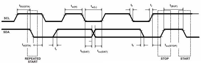 Figure 1. I2C-Compatible Interface Timing Diagrams