ZHCSE45C July   2015  – May 2018

PRODUCTION DATA.  

  1. 特性
  2. 应用
  3. 说明
    1.     简化原理图
  4. 修订历史记录
  5. 说明 (续)
  6. Device Comparison Table
  7. Pin Configuration and Functions
    1.     Pin Functions
  8. Specifications
    1. 8.1 Absolute Maximum Ratings
    2. 8.2 ESD Ratings
    3. 8.3 Recommended Operating Conditions
    4. 8.4 Thermal Information
    5. 8.5 Electrical Characteristics
    6. 8.6 Timing Requirements
    7. 8.7 Typical Characteristics
  9. Detailed Description
    1. 9.1 Functional Block Diagram
    2. 9.2 Feature Description
      1. 9.2.1  Device Power-On-Reset (POR)
      2. 9.2.2  Device Power Up from Battery without Input Source
      3. 9.2.3  Device Power Up from Input Source
        1. 9.2.3.1 Power Up REGN Regulation (LDO)
        2. 9.2.3.2 Poor Source Qualification
        3. 9.2.3.3 Input Source Type Detection
          1. 9.2.3.3.1 PSEL Pins Set Input Current Limit
          2. 9.2.3.3.2 Force Input Current Limit Detection
        4. 9.2.3.4 Input Voltage Limit Threshold Setting (VINDPM Threshold)
        5. 9.2.3.5 Converter Power-Up
      4. 9.2.4  Input Current Optimizer (ICO)
      5. 9.2.5  Boost Mode Operation from Battery
      6. 9.2.6  Power Path Management
        1. 9.2.6.1 Narrow VDC Architecture
        2. 9.2.6.2 Dynamic Power Management
        3. 9.2.6.3 Supplement Mode
      7. 9.2.7  Battery Charging Management
        1. 9.2.7.1 Autonomous Charging Cycle
        2. 9.2.7.2 Battery Charging Profile
        3. 9.2.7.3 Charging Termination
        4. 9.2.7.4 Resistance Compensation (IRCOMP)
        5. 9.2.7.5 Thermistor Qualification
          1. 9.2.7.5.1 JEITA Guideline Compliance in Charge Mode
          2. 9.2.7.5.2 Cold/Hot Temperature Window in Boost Mode
        6. 9.2.7.6 Charging Safety Timer
      8. 9.2.8  Battery Monitor
      9. 9.2.9  Status Outputs (PG, STAT, and INT)
        1. 9.2.9.1 Power Good Indicator (PG)
        2. 9.2.9.2 Charging Status Indicator (STAT)
        3. 9.2.9.3 Interrupt to Host (INT)
      10. 9.2.10 BATET (Q4) Control
        1. 9.2.10.1 BATFET Disable Mode (Shipping Mode)
        2. 9.2.10.2 BATFET Enable (Exit Shipping Mode)
        3. 9.2.10.3 BATFET Full System Reset
      11. 9.2.11 Current Pulse Control Protocol
      12. 9.2.12 Input Current Limit on ILIM
      13. 9.2.13 Thermal Regulation and Thermal Shutdown
        1. 9.2.13.1 Thermal Protection in Buck Mode
        2. 9.2.13.2 Thermal Protection in Boost Mode
      14. 9.2.14 Voltage and Current Monitoring in Buck and Boost Mode
        1. 9.2.14.1 Voltage and Current Monitoring in Buck Mode
          1. 9.2.14.1.1 Input Overvoltage (ACOV)
          2. 9.2.14.1.2 System Overvoltage Protection (SYSOVP)
        2. 9.2.14.2 Current Monitoring in Boost Mode
          1. 9.2.14.2.1 VBUS Overcurrent Protection
          2. 9.2.14.2.2 Boost Mode Overvoltage Protection
      15. 9.2.15 Battery Protection
        1. 9.2.15.1 Battery Overvoltage Protection (BATOVP)
        2. 9.2.15.2 Battery Over-Discharge Protection
        3. 9.2.15.3 System Overcurrent Protection
      16. 9.2.16 Serial Interface
        1. 9.2.16.1 Data Validity
        2. 9.2.16.2 START and STOP Conditions
        3. 9.2.16.3 Byte Format
        4. 9.2.16.4 Acknowledge (ACK) and Not Acknowledge (NACK)
        5. 9.2.16.5 Slave Address and Data Direction Bit
        6. 9.2.16.6 Single Read and Write
        7. 9.2.16.7 Multi-Read and Multi-Write
    3. 9.3 Device Functional Modes
      1. 9.3.1 Host Mode and Default Mode
    4. 9.4 Register Maps
      1. 9.4.1  REG00
        1. Table 6. REG00
      2. 9.4.2  REG01
        1. Table 7. REG01
      3. 9.4.3  REG02
        1. Table 8. REG02
      4. 9.4.4  REG03
        1. Table 9. REG03
      5. 9.4.5  REG04
        1. Table 10. REG04
      6. 9.4.6  REG05
        1. Table 11. REG05
      7. 9.4.7  REG06
        1. Table 12. REG06
      8. 9.4.8  REG07
        1. Table 13. REG07
      9. 9.4.9  REG08
        1. Table 14. REG08
      10. 9.4.10 REG09
        1. Table 15. REG09
      11. 9.4.11 REG0A
        1. Table 16. REG0A
      12. 9.4.12 REG0B
        1. Table 17. REG0B
      13. 9.4.13 REG0C
        1. Table 18. REG0C
      14. 9.4.14 REG0D
        1. Table 19. REG0D
      15. 9.4.15 REG0E
        1. Table 20. REG0E
      16. 9.4.16 REG0F
        1. Table 21. REG0F
      17. 9.4.17 REG10
        1. Table 22. REG10
      18. 9.4.18 REG11
        1. Table 23. REG11
      19. 9.4.19 REG12
        1. Table 24. REG12
      20. 9.4.20 REG13
        1. Table 25. REG13
      21. 9.4.21 REG14
        1. Table 26. REG14
  10. 10Application and Implementation
    1. 10.1 Application Information
    2. 10.2 Typical Application
      1. 10.2.1 Design Requirements
      2. 10.2.2 Detailed Design Procedure
        1. 10.2.2.1 Inductor Selection
        2. 10.2.2.2 Buck Input Capacitor
        3. 10.2.2.3 System Output Capacitor
      3. 10.2.3 Application Curves
    3. 10.3 System Examples
  11. 11Power Supply Recommendations
  12. 12Layout
    1. 12.1 Layout Guidelines
    2. 12.2 Layout Example
  13. 13器件和文档支持
    1. 13.1 文档支持
      1. 13.1.1 相关文档
    2. 13.2 接收文档更新通知
    3. 13.3 社区资源
    4. 13.4 商标
    5. 13.5 静电放电警告
    6. 13.6 术语表
  14. 14机械、封装和可订购信息

封装选项

机械数据 (封装 | 引脚)
散热焊盘机械数据 (封装 | 引脚)
订购信息

Application Curves

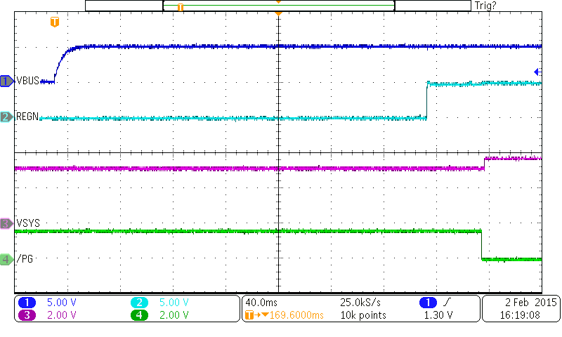
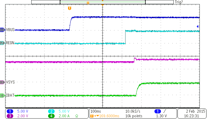
bq25896 wvfrm_02_pwr_up_chrg_dsbl_slusbu7.png
VBAT = 3.2 V
Figure 47. Power Up with Charge Disabled
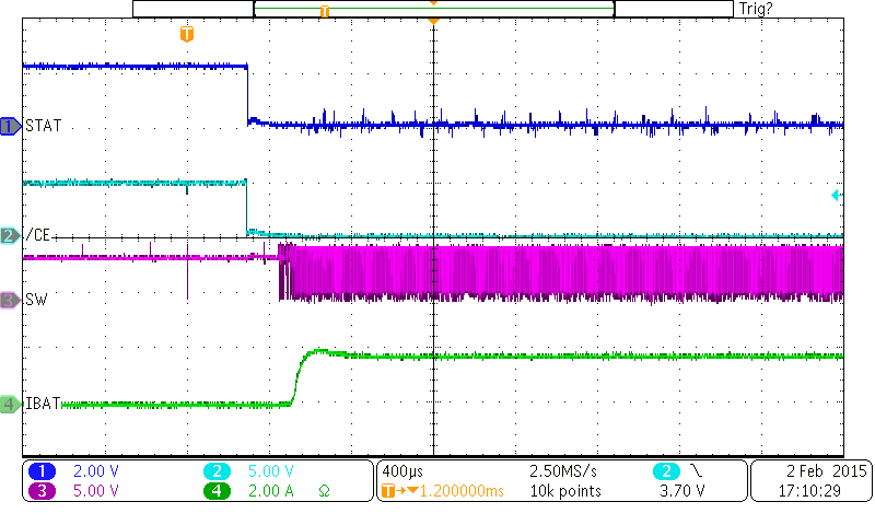
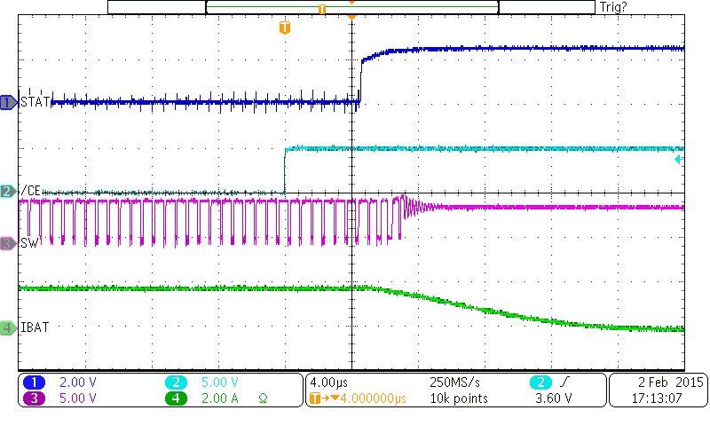
bq25896 wvfrm_04_chrg_enbl_5v_slusbu7.png
VBUS = 5 V
Figure 49. Charge Enable
bq25896 wvfrm_06_inp_dpm_rspn_slusbu7.png
VBUS = 5 V IIN = 3 A Charge Disable
Figure 51. Input Current DPM Response without Battery
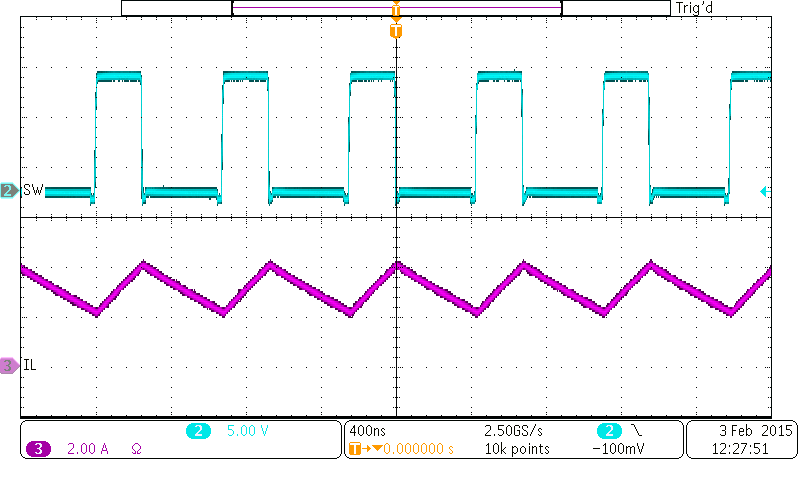
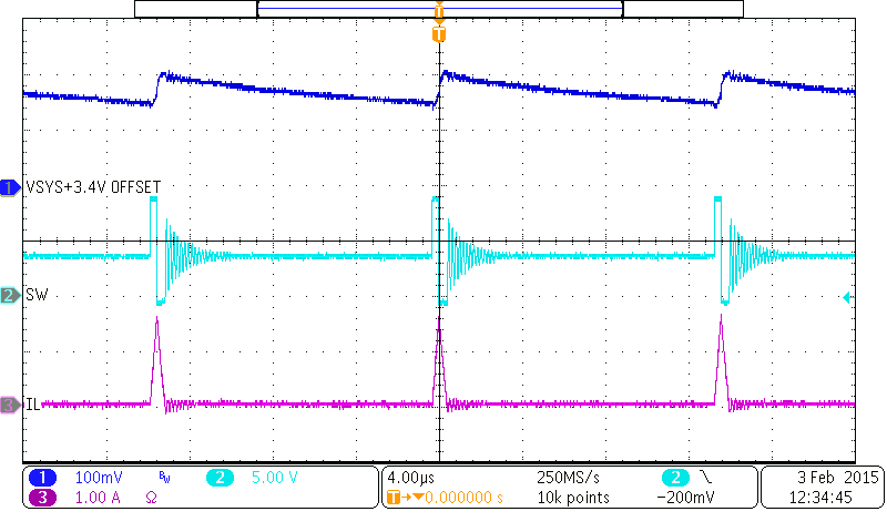
bq25896 wvfrm_08_pwm_swtch_slusbu7.png
VBUS = 12 V VBAT = 3.8 V ICHG = 3 A
Figure 53. PWM Switching Waveform
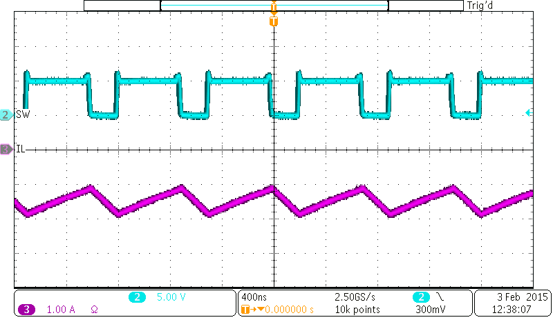
bq25896 wvfrm_10_boost_mode_swtch_slusbu7.png
VBAT = 3.8 V ILOAD = 1 A
Figure 55. Boost Mode Switching Waveform
bq25896 wvfrm_03_pwr_up_chrg_enbl_slusbu7.png
Figure 48. Power Up with Charge Enabled
bq25896 wvfrm_05_chrg_dsbl_12v_slusbu7.png
VBUS = 12 V
Figure 50. Charge Disable
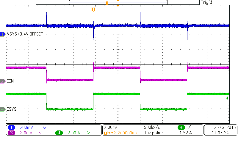
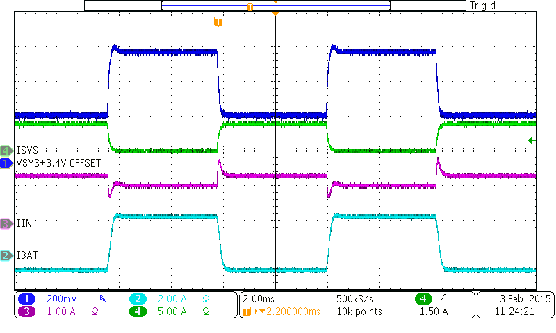
bq25896 wvfrm_07_load_trns_supp_slusbu7.png
VBUS = 9 V IIN = 1.5 A VBAT = 3.8 V
ICHG = 2 A ISYS = 0 A - 4 A
Figure 52. Load Transient During Supplement Mode
bq25896 wvfrm_09_pfm_swtch_slusbu7.png
VBUS = 9V ISYS = 10 mA, Charge Disable
No Battery
Figure 54. PFM Switching Waveform
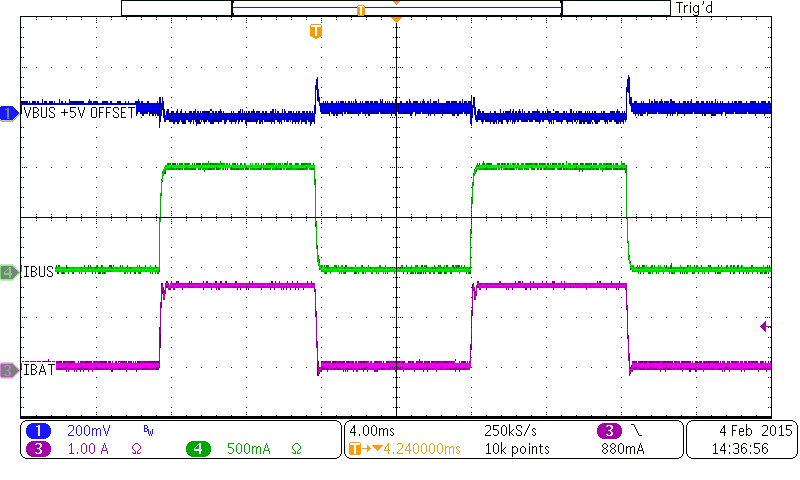
bq25896 wvfrm_11_boost_mode_load_trns_slusbu7.png
VBAT = 3.8 V ILOAD = 0 A - 1 A
Figure 56. Boost Mode Load Transient