ZHCSDX5C July   2015  – October 2022 BQ25895M

PRODUCTION DATA  

  1. 特性
  2. 应用
  3. 说明
  4. Revision History
  5. 说明(续)
  6. Pin Configuration and Functions
  7. Specifications
    1. 7.1 Absolute Maximum Ratings
    2. 7.2 ESD Ratings
    3. 7.3 Recommended Operating Conditions
    4. 7.4 Thermal Information
    5. 7.5 Electrical Characteristics
    6. 7.6 Timing Requirements
    7. 7.7 Typical Characteristics
  8. Detailed Description
    1. 8.1 Functional Block Diagram
    2. 8.2 Feature Description
      1. 8.2.1  Device Power-On-Reset (POR)
      2. 8.2.2  Device Power Up from Battery without Input Source
      3. 8.2.3  Device Power Up from Input Source
        1. 8.2.3.1 Power Up REGN Regulation (LDO)
        2. 8.2.3.2 Poor Source Qualification
        3. 8.2.3.3 Input Source Type Detection
          1. 8.2.3.3.1 D+/D– Detection Sets Input Current Limit
          2. 8.2.3.3.2 Force Input Current Limit Detection
        4. 8.2.3.4 Input Voltage Limit Threshold Setting (VINDPM Threshold)
        5. 8.2.3.5 Converter Power-Up
      4. 8.2.4  Input Current Optimizer (ICO)
      5. 8.2.5  Boost Mode Operation from Battery
      6. 8.2.6  Power Path Management
        1. 8.2.6.1 Narrow VDC Architecture
        2. 8.2.6.2 Dynamic Power Management
        3. 8.2.6.3 Supplement Mode
      7. 8.2.7  Battery Charging Management
        1. 8.2.7.1 Autonomous Charging Cycle
        2. 8.2.7.2 Battery Charging Profile
        3. 8.2.7.3 Charging Termination
        4. 8.2.7.4 Resistance Compensation (IRCOMP)
        5. 8.2.7.5 Thermistor Qualification
          1. 8.2.7.5.1 Cold/Hot Temperature Window in Charge Mode
          2. 8.2.7.5.2 Cold/Hot Temperature Window in Boost Mode
        6. 8.2.7.6 Charging Safety Timer
      8. 8.2.8  Battery Monitor
      9. 8.2.9  Status Outputs (STAT, and INT)
        1. 8.2.9.1 Charging Status Indicator (STAT)
        2. 8.2.9.2 Interrupt to Host (INT)
      10. 8.2.10 BATET (Q4) Control
        1. 8.2.10.1 BATFET Disable Mode (Shipping Mode)
        2. 8.2.10.2 BATFET Enable (Exit Shipping Mode)
        3. 8.2.10.3 BATFET Full System Reset
      11. 8.2.11 Current Pulse Control Protocol
      12. 8.2.12 Input Current Limit on ILIM
      13. 8.2.13 Thermal Regulation and Thermal Shutdown
        1. 8.2.13.1 Thermal Protection in Buck Mode
        2. 8.2.13.2 Thermal Protection in Boost Mode
      14. 8.2.14 Voltage and Current Monitoring in Buck and Boost Mode
        1. 8.2.14.1 Voltage and Current Monitoring in Buck Mode
          1. 8.2.14.1.1 Input Overvoltage (ACOV)
          2. 8.2.14.1.2 System Overvoltage Protection (SYSOVP)
        2. 8.2.14.2 Current Monitoring in Boost Mode
          1. 8.2.14.2.1 Boost Mode Overvoltage Protection
      15. 8.2.15 Battery Protection
        1. 8.2.15.1 Battery Overvoltage Protection (BATOVP)
        2. 8.2.15.2 Battery Over-Discharge Protection
        3. 8.2.15.3 System Overcurrent Protection
      16. 8.2.16 Serial Interface
        1. 8.2.16.1 Data Validity
        2. 8.2.16.2 START and STOP Conditions
        3. 8.2.16.3 Byte Format
        4. 8.2.16.4 Acknowledge (ACK) and Not Acknowledge (NACK)
        5. 8.2.16.5 Target Address and Data Direction Bit
        6. 8.2.16.6 Single Read and Write
        7. 8.2.16.7 Multi-Read and Multi-Write
    3. 8.3 Device Functional Modes
      1. 8.3.1 Host Mode and Default Mode
    4. 8.4 Register Maps
      1. 8.4.1  REG00
      2. 8.4.2  REG01
      3. 8.4.3  REG02
      4. 8.4.4  REG03
      5. 8.4.5  REG04
      6. 8.4.6  REG05
      7. 8.4.7  REG06
      8. 8.4.8  REG07
      9. 8.4.9  REG08
      10. 8.4.10 REG09
      11. 8.4.11 REG0A
      12. 8.4.12 REG0B
      13. 8.4.13 REG0C
      14. 8.4.14 REG0D
      15. 8.4.15 REG0E
      16. 8.4.16 REG0F
      17. 8.4.17 REG10
      18. 8.4.18 REG11
      19. 8.4.19 REG12
      20. 8.4.20 REG13
      21. 8.4.21 REG14
  9. Application and Implementation
    1. 9.1 Application Information
    2. 9.2 Typical Application
      1. 9.2.1 Design Requirements
      2. 9.2.2 Detailed Design Procedure
        1. 9.2.2.1 Inductor Selection
        2. 9.2.2.2 Buck Input Capacitor
        3. 9.2.2.3 System Output Capacitor
      3. 9.2.3 Application Curves
    3. 9.3 System Examples
  10. 10Power Supply Recommendations
  11. 11Layout
    1. 11.1 Layout Guidelines
    2. 11.2 Layout Example
  12. 12Device and Documentation Support
    1. 12.1 Device Support
      1. 12.1.1 第三方产品免责声明
    2. 12.2 Documentation Support
      1. 12.2.1 Related Documentation
    3. 12.3 接收文档更新通知
    4. 12.4 支持资源
    5. 12.5 Trademarks
    6. 12.6 Electrostatic Discharge Caution
    7. 12.7 术语表
  13. 13Mechanical, Packaging, and Orderable Information

封装选项

机械数据 (封装 | 引脚)
散热焊盘机械数据 (封装 | 引脚)
订购信息
Cold/Hot Temperature Window in Charge Mode

The device continuously monitors battery temperature by measuring the voltage between the TS pins and ground, typically determined by a negative temperature coefficient thermistor (NTC) and an external voltage divider. The device compares this voltage against its internal thresholds to determine if charging is allowed. To initiate a charge cycle, the battery temperature must be within the VLTF to VHTF thresholds. During the charge cycle the battery temperature must be within the VLTF to VTCO thresholds, else the device suspends charging and waits until the battery temperature is within the VLTF to VHTF range.

GUID-20201116-CA0I-P0X1-XGWQ-VXNDQHPVKR51-low.gif Figure 8-6 TS Resistor Network

When the TS fault occurs, the fault register REG0C[2:0] indicates the actual condition on each TS pin and an INT is asserted to the host. The STAT pin indicates the fault when charging is suspended.

GUID-78CCC1DD-96A2-4F28-B12A-B8E302AC0E69-low.gifFigure 8-7 TS Pin Thermistor Sense Thresholds

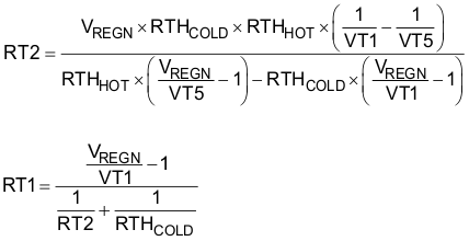
Assuming a 103AT NTC thermistor on the battery pack as shown in Figure 8-6, the value RT1 and RT2 can be determined by using Equation 2:

Equation 2. GUID-709D9D8A-A47E-43DA-B9A0-97250137A3BC-low.gif

Select 0°C to 45°C range for Li-ion or Li-polymer battery,
RTHCOLD = 27.28 kΩ
RTHHOT = 4.91 kΩ
RT1 = 5.21 kΩ
RT2 = 29.87 kΩ