ZHCSFK5 October 2016
PRODUCTION DATA.
- 1 特性
- 2 应用
- 3 说明
- 4 修订历史记录
- 5 Pin Configuration and Functions
- 6 Specifications
- 7 Typical Characteristics
-
8 Detailed Description
- 8.1 Overview
- 8.2 Functional Block Diagram
- 8.3
Feature Description
- 8.3.1 Device Power Up
- 8.3.2 Battery Switch (Q1 + Q2)
- 8.3.3 Integrated 10-bit ADC for Monitoring
- 8.3.4 Linear Regulation Mode (LDO)
- 8.3.5
Protection Features
- 8.3.5.1 Reverse Current Protection (RCP)
- 8.3.5.2 Internal Thermal Shutdown
- 8.3.5.3 Input Overvoltage Protection
- 8.3.5.4 IBUS and VBUS Protection
- 8.3.5.5 IBAT and VBAT Protection
- 8.3.5.6 VOUT Protection
- 8.3.5.7 VDROP Protection
- 8.3.5.8 VBUS Temperature (TS_BUS_FLT) and Battery Temperature (TS_BAT_FLT)
- 8.3.6 I2C Serial Interface
- 8.4 Device Functional Modes
- 8.5
I2C Register Maps
- 8.5.1 I2C Register Summary Table
- 8.5.2 REG00 (DEVICE_INFO)
- 8.5.3 REG01 (EVENT_1_MASK)
- 8.5.4 REG02 (EVENT_2_MASK)
- 8.5.5 REG03 (EVENT_1)
- 8.5.6 REG04 (EVENT_2)
- 8.5.7 REG05 (EVENT_1_EN)
- 8.5.8 REG06 (CONTROL)
- 8.5.9 REG07 (ADC_CONTROL)
- 8.5.10 REG08 (ADC_EN)
- 8.5.11 REG09 (PROTECTION)
- 8.5.12 REG0A (VBUS_OVP)
- 8.5.13 REG0B (VOUT_REG)
- 8.5.14 REG0C (VDROP_OVP)
- 8.5.15 REG0D (VDROP_ALM)
- 8.5.16 REG0E (VBAT_REG)
- 8.5.17 REG0F (IBAT_REG)
- 8.5.18 REG10 (IBUS_REG)
- 8.5.19 REG11 (TS_BUS_FLT)
- 8.5.20 REG12 (TS_BAT_FLT)
- 8.5.21 REG 13 and REG 14 (VBUS_ADC)
- 8.5.22 REG15 and REG16 (IBUS_ADC)
- 8.5.23 REG17 and REG18 (VOUT_ADC)
- 8.5.24 REG19 and REG1A (VDROP_ADC)
- 8.5.25 REG1B and REG1C (VBAT_ADC)
- 8.5.26 REG1D and REG1E (IBAT_ADC)
- 8.5.27 REG1F and REG20 (TS_BUS_ADC)
- 8.5.28 REG21 and REG22 (TS_BAT_ADC)
- 8.5.29 REG 23 (TDIE_ADC)
- 8.5.30 REG 24 (EVENT_2_EN)
- 8.5.31 REG 25 (EVENT_3_MASK)
- 8.5.32 REG 26 (EVENT_3)
- 8.5.33 REG27 and REG28 (VUSB_ADC)
- 8.5.34 REG 29 (CONTROL_2)
- 8.5.35 REG 40 (DIE_TEMP_FLT)
- 9 Application and Implementation
- 10Power Supply Recommendations
- 11Layout
- 12器件和文档支持
- 13机械、封装和可订购信息
9 Application and Implementation
NOTE
Information in the following applications sections is not part of the TI component specification, and TI does not warrant its accuracy or completeness. TI’s customers are responsible for determining suitability of components for their purposes. Customers should validate and test their design implementation to confirm system functionality.
9.1 Application Information
A typical application consists of the device configured as an I2C controlled device and another switch mode charger for Li-Ion and Li-polymer batteries used in a wide range of smart phones and other portable devices. A host controls which charger is enabled during the charging process.
9.2 Typical Application
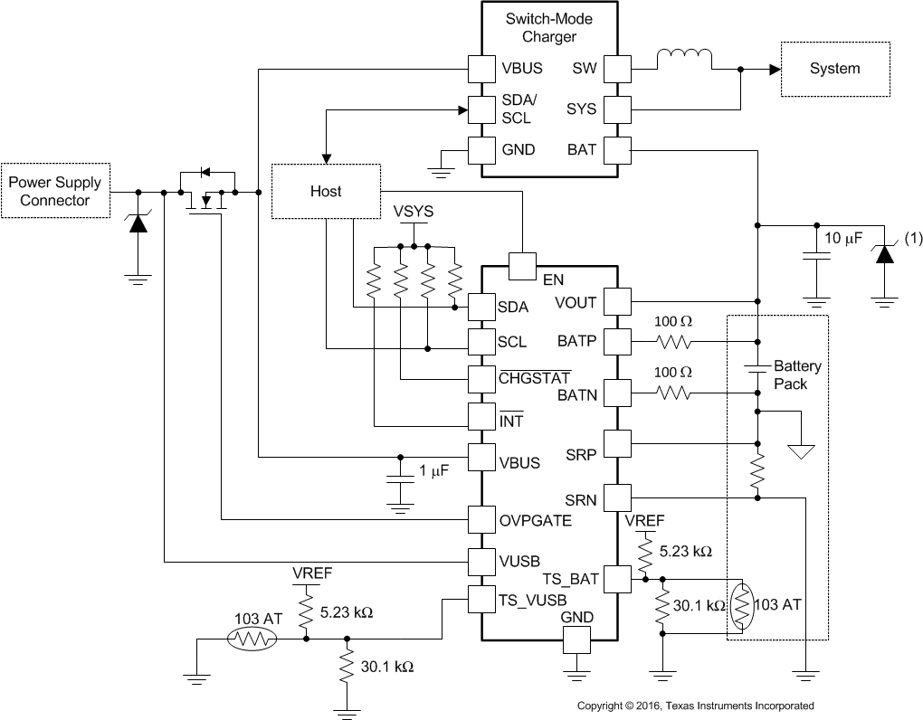 Figure 55. bq25872 Typical Application
9.2.1 Design Requirements
Table 37. Design Requirement
| PARAMETER | VALUE |
|---|---|
| Input voltage range | 3 V to 6 V |
| Input current limit | 0.1 A to 7.5 A |
| Output voltage range | 3 V to 4.975 V |
9.2.2 Detailed Design Procedure
The bq25872 continuously monitors battery and adaptor connector temperature by measuring the voltage between TS_BAT pin and TS_BUS pins and ground, typically determined by a negative temperature coefficient thermistor and an external voltage divider. The device compares this voltage against its internal thresholds to determine if charging is allowed. To initiate a charging cycle, both battery and connector temperatures must be lower than the temperature threshold, else the device suspends charging and waits until both temperatures are blow the threshold.
Assuming a 103 AT NTC thermistor is used on the battery pack, the values RT1 (connected between TS_X pin to VREF) and RT2 (connected between TS_X and ground) can be determined by using the following equations.

where
- RTHcold and VLTF are the resistance of NTC under the cold temperature and the corresponding TS_X pin voltage when charge is allowed, RTHhot and VTCOare the resistance of NTC under the hot temperature and the corresponding TS_X pin voltage when charge is allowed.
9.2.3 Application Curves
