ZHCSJD3C july 2018 – april 2023 BQ25150
PRODUCTION DATA
- 1
- 1 特性
- 2 应用
- 3 说明
- 4 Revision History
- 5 说明(续)
- 6 Device Key Default Settings
- 7 Pin Configuration and Functions
- 8 Specifications
-
9 Detailed Description
- 9.1 Overview
- 9.2 Functional Block Diagram
- 9.3
Feature Description
- 9.3.1 Linear Charger and Power Path
- 9.3.2 Protection Mechanisms
- 9.3.3 ADC
- 9.3.4 VDD LDO
- 9.3.5 Load Switch / LDO Output and Control
- 9.3.6 PMID Power Control
- 9.3.7 MR Wake and Reset Input
- 9.3.8 14-Second Watchdog for HW Reset
- 9.3.9 Faults Conditions and Interrupts ( INT)
- 9.3.10 Power Good ( PG) Pin
- 9.3.11 External NTC Monitoring (TS)
- 9.3.12 External NTC Monitoring (ADCIN)
- 9.3.13 I2C Interface
- 9.4 Device Functional Modes
- 9.5 Register Map
- 10Application and Implementation
- 11Power Supply Recommendations
- 12Layout
- 13Device and Documentation Support
- 14Mechanical, Packaging, and Orderable Information
7 Pin Configuration and Functions
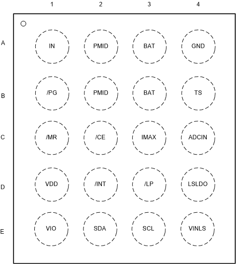
 Figure 7-1 YFP Package20-Pin DSBGATop View
Table 7-1 Pin Functions
| PIN | I/O | DESCRIPTION | |
|---|---|---|---|
| NAME | NO. | ||
| IN | A1 | I | DC Input Power Supply. IN is connected to the external DC supply. Bypass IN to GND with at least 1 µF of capacitance using a ceramic capacitor. |
| PMID | A2, B2 | I/O | High Side Bypass Connection. Connect at least 10-µF ceramic capacitor (at least 3 µF of ceramic capacitance with DC bias de-rating) from PMID to GND as close to the PMID and GND pins as possible. Note: Shorting PMID to IN pin is not recommended as it may cause large discharge current from battery to IN if IN pin is not truly floating. |
| GND | A4 | PWR | Ground connection. Connect to the ground plane of the circuit. |
| VDD | D1 | O | Digital supply LDO. Connect at least 4.7-µF capacitor to ground. |
| CE | C2 | I | Charge Enable. Drive CE low or leave disconnected to enable charging when VIN is valid. Drive CE high to disable charge when VIN is present. CE is pulled low internally with 900-kΩ resistor. CE has no effect when VIN is not present. |
| SCL | E3 | I/O | I2C Interface Clock. Connect SCL to the logic rail through a 10-kΩ resistor. |
| SDA | E2 | I | I2C Interface Data. Connect SDA to the logic rail through a 10-kΩ resistor. |
| LP | D3 | I | Low Power Mode Enable. Drive this pin low to set the device in low power mode when powered by the battery. This pin must be driven high to allow I2C communication when VIN is not present. LP is pulled low internally with 900-kΩ resistor. This pin has no effect when VIN is present. |
| IMAX | C3 | I | Connect a 10-kΩ or lower resistor to this pin to set the maximum allowable fast charge current. Must not be left floating. |
| INT | D2 | O | INT is an open-drain output that signals fault interrupts. When a fault occurs, a 128-µs pulse is sent out as an interrupt for the host. INT is enabled/disabled using the MASK_INT bit in the control register. |
| ADCIN | C4 | I | Input Channel to the ADC. Maximum ADC range 1.2 V. Leave floating or connect to ground if not used. |
| MR | C1 | I | Manual Reset Input. MR is a general purpose input that must be held low for greater than tHWRESET to go into HW Reset and power cycle the output rails. If MR is also used to wake up the device out of Ship Mode when pressed for at least tWAKE2. MR has in internal 125-kΩ pull-up resistor to BAT. |
| LS/LDO | D4 | O | Load Switch or LDO output. Connect 2.2 µF of ceramic capacitance to this pin to assure stability. Be sure to account for capacitance bias voltage derating when selecting the capacitor. If LDO is not to be used,, the pin may be shorted to VINLS |
| VINLS | E4 | I | Input to the Load Switch / LDO output. Connect at least 1 µF of ceramic capacitance from this pin to ground. |
| BAT | A3, B3 | I/O | Battery Connection. Connect to the positive terminal of the battery. Bypass BAT to GND with at least 1 µF of ceramic capacitance. |
| TS | B4 | I | Battery Pack NTC Monitor. Connect TS to a 10-kΩ NTC Thermistor in parallel to a 10-kΩ resistor. If TS function is not to be used connect a 5-kΩ resistor from TS to ground. |
| PG | B1 | O | Open-drain Power Good status indication output. PG is pulled to GND when VIN is above VBAT+ VSLP and less than VOVP. PG is high-impedance when the input power is not within specified limits. Connect PG to the desired logic voltage rail using a 1-kΩ to 100-kΩ resistor, or use with an LED for visual indication. PG can also be configured through I2C as a push-button level shifted output ( MR), where the output of the PG pin reflects the status of the MR input, but pulled up to the desired logic voltage rail using a 1-kΩ to 100-kΩ resistor. The PG pin can also be configured as a general purpose open drain output. |
| VIO | E1 | I | System IO supply. Connect to system IO supply to allow level shifting of input signals (SDA, SCL, LP and CE) to the device internal digital domain. Connect to VDD when external IO supply is not available. |