ZHCS958G June   2012  – September 2017 BQ24392

PRODUCTION DATA.  

  1. 特性
  2. 应用
  3. 说明
  4. 修订历史记录
  5. Pin Configuration and Functions
  6. Specifications
    1. 6.1 Absolute Maximum Ratings
    2. 6.2 ESD Ratings
    3. 6.3 Recommended Operating Conditions
    4. 6.4 Thermal Information
    5. 6.5 Electrical Characteristics
    6. 6.6 Typical Characteristics
  7. Detailed Description
    1. 7.1 Overview
    2. 7.2 Functional Block Diagram
    3. 7.3 Feature Description
      1. 7.3.1 Charger Detection
    4. 7.4 Device Functional Modes
  8. Application and Implementation
    1. 8.1 Application Information
      1. 8.1.1 Using the BQ24392 GPIOs
        1. 8.1.1.1 CHG_AL and CHG_DET
        2. 8.1.1.2 SW_OPEN
        3. 8.1.1.3 GOOD_BAT
        4. 8.1.1.4 Slow Plug-in Event
    2. 8.2 Typical Application
      1. 8.2.1 Design Requirements
      2. 8.2.2 Detailed Design Procedure
      3. 8.2.3 Application Curves
  9. Power Supply Recommendations
  10. 10Layout
    1. 10.1 Layout Guidelines
    2. 10.2 Layout Example
  11. 11器件和文档支持
    1. 11.1 接收文档更新通知
    2. 11.2 社区资源
    3. 11.3 商标
    4. 11.4 静电放电警告
  12. 12机械、封装和可订购信息

封装选项

机械数据 (封装 | 引脚)
散热焊盘机械数据 (封装 | 引脚)
订购信息

Specifications

Absolute Maximum Ratings

over –40℃ to 85℃ temperature range (unless otherwise noted)
MIN MAX UNIT
Input Voltage VBUS –2 28 V
CHG_AL_N –2 28 V
DM_HOST –0.3 7 V
DP_HOST –0.3 7
GOOD_BAT –0.3 7
DP_CON –0.3 7
DM_CON –0.3 7
CHG_DET –0.3 7
Tstg Storage temperature range 65 150 °C

ESD Ratings

VALUE UNIT
V(ESD) Electrostatic discharge Human-body model (HBM), per ANSI/ESDA/JEDEC JS-001(1) ±4000 V
Charged-device model (CDM), per JEDEC specification JESD22-C101(2) ±1500
IEC Contact discharge pins DP_CON and DM_CON to GND ±8000
JEDEC document JEP155 states that 500-V HBM allows safe manufacturing with a standard ESD control process. Manufacturing with less than 500-V HBM is possible with the necessary precautions.
JEDEC document JEP157 states that 250-V CDM allows safe manufacturing with a standard ESD control process. Manufacturing with less than 250-V CDM is possible with the necessary precautions.

Recommended Operating Conditions

MIN MAX UNIT
VBUS 4.75 5.25 V
GOOD_BAT 0 VBUS
DM_HOST 0 3.6
DP_HOST 0 3.6
DM_CON 0 3.6
DP_CON 0 3.6

Thermal Information

THERMAL METRIC(1) bq24392 UNIT
RSE
10 PINS
RθJA Junction-to-ambient thermal resistance 167.7 °C/W
RθJC(top) Junction-to-case (top) thermal resistance 78.8 °C/W
RθJB Junction-to-board thermal resistance 95.8 °C/W
ψJT Junction-to-top characterization parameter 4.7 °C/W
ψJB Junction-to-board characterization parameter 95.9 °C/W
For more information about traditional and new thermal metrics, see the Semiconductor and IC Package Thermal Metrics application report.

Electrical Characteristics

VBUS = 4.5 V to 5.5 V, TA = –40°C to 85°C (unless otherwise noted)(1)
PARAMETER TEST CONDITIONS MIN TYP MAX UNIT
VVBUS_VALID VBUS Valid threshold Rising VBUS threshold 3.5 V
VOH CHG_DET CHG_DET IOH = –2 mA 3.5 VBUS V
VOL CHG_DET, SW_OPEN, CHG_AL_N CHG_DET, SW_OPEN, CHG_AL_N IOL = 2 mA 0.4 V
VIH High-level input voltage GOOD_BAT 1.1 V
VIL Low-level input voltage 0.5 V
RPD Internal pull-down resistance 950
tDBP Dead battery provision timer 32 45 Mins
VUSBIO ON- state resistance match between DM_CON, DP_CON, DM_HOST, DP_HOST 0 3.6 V
RON ON-state resistance VDM_HOST and VDP_HOST = 0 to 3.6 V, IDP_CON and IDM_CON = –2 mA 3.5 6.9 Ω
RON(flat) ON-state resistance flatness 1.1 Ω
ΔRON ON- state resistance match between channels VDM_HOST and VDP_HOST = 0.4 V, IDP_CON and IDM_CON = –2 mA 0.5 Ω
ICC-SW (ON) Current consumption VVBUS = 5V,
VIH(GOOD_BAT)= 1.1 V
250 µA
VVBUS = 5 V,
VIH(GOOD_BAT) = 2.5 V
80 µA
ICC-SW (OFF) Current consumption with USB switch off VVBUS = 5 V; USB Switch OFF 45 µA
IUSBI/O (ON) Leakage current with USB switch on VDM_HOST and VDP_HOST = 0 to 3.6 V, IDP_CON and IDM_CON = –2 mA 50 nA
IUSBI/O (OFF) Leakage current with USB switch off 45 nA
CI(OFF) Capacitance with USB switch off DP_HOST, DM_HOST DC bias = 0 V or 3.6 V, f = 10 MHz 2 pF
CO(OFF) Capacitance with USB switch off DP_CON, DM_CON 10 pF
CI(ON) Capacitance with USB switch on DP_HOST, DM_HOST 11 pF
CO(ON) Capacitance with USB switch on DP_CON, DM_CON 11 pF
BW Bandwidth RL = 50 Ω, Switch ON 920 MHz
OISO Isolation with USB switch off f = 240 MHz, RL = 50 Ω, Switch OFF –26 dB
XTALK Crosstalk f = 240 MHz, RL = 50 Ω –30.5 dB
CHG_DET max value will be clamped at 7 V when VVBUS > 7 V

Typical Characteristics

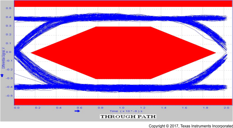
BQ24392 eye1_lis146.gif
Figure 1. 480-Mbps USB 2.0 Eye Diagram with No Device
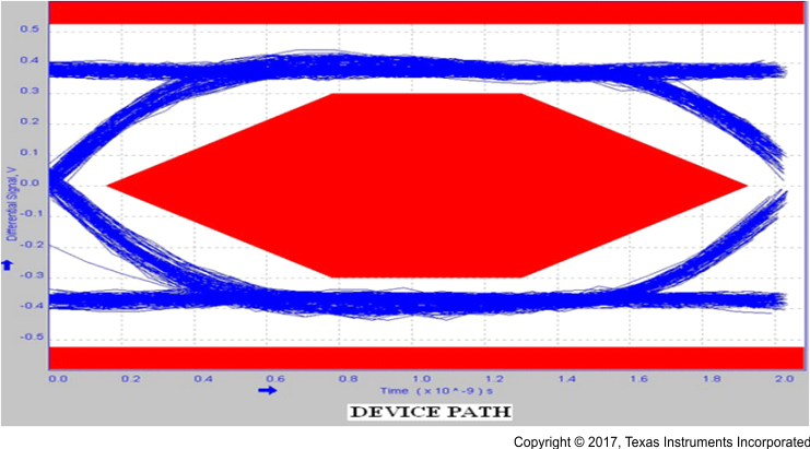
BQ24392 eye2_lis146.gif
Figure 2. 480-Mbps USB 2.0 Eye Diagram with USB Switch