ZHCSGY5A October 2017 – December 2017
PRODUCTION DATA.
- 1 特性
- 2 应用范围
- 3 说明
- 4 修订历史记录
- 5 说明 (续)
- 6 Device Comparison Table
- 7 Pin Configuration and Functions
- 8 Specifications
- 9 Detailed Description
- 10Application and Implementation
- 11Power Supply Recommendations
- 12Layout
- 13器件和文档支持
- 14机械、封装和可订购信息
9.3.6 Battery Pack Temperature Monitoring
The bq2407x features an external battery pack temperature monitoring input. The TS input connects to the NTC thermistor in the battery pack to monitor battery temperature and prevent dangerous over-temperature conditions. During charging, INTC is sourced to TS and the voltage at TS is continuously monitored. If, at any time, the voltage at TS is outside of the operating range (VCOLD to VHOT), charging is suspended. The timers maintain their values but suspend counting. When the voltage measured at TS returns to within the operation window, charging is resumed and the timers continue counting. When charging is suspended due to a battery pack temperature fault, the CHG pin remains low and continues to indicate charging.
For applications that do not require the TS monitoring function, connect a 10-kΩ resistor from TS to VSS to set the TS voltage at a valid level and maintain charging.
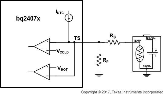
The allowed temperature range for 103AT-2 type thermistor is 0°C to 50°C. However, the user may increase the range by adding two external resistors. See Figure 20 for the circuit details. The values for Rs and Rp are calculated using the following equations:


where
- RTH: Thermistor Hot Trip Value found in thermistor data sheet
- RTC: Thermistor Cold Trip Value found in thermistor data sheet
- VH: IC's Hot Trip Threshold = 0.3 V nominal
- VC: IC's Cold Trip Threshold = 2.1 V nominal
- ITS: IC's Output Current Bias = 75 µA nominal
- NTC Thermsitor Semitec 103AT-4
Rs and Rp 1% values were chosen closest to calculated values in Table 3.
Table 3. Calculated Values
| COLD TEMP RESISTANCE AND TRIP THRESHOLD, Ω (°C) | HOT TEMP RESISTANCE AND TRIP THRESHOLD, Ω (°C) | EXTERNAL BIAS RESISTOR, Rs (Ω) | EXTERNAL BIAS RESISTOR, Rp (Ω) |
|---|---|---|---|
| 28000 (–0.6) | 4000 (51) | 0 | ∞ |
| 28480 (–1) | 3536 (55) | 487 | 845000 |
| 28480 (–1) | 3021 (60) | 1000 | 549000 |
| 33890 (–5) | 4026 (51) | 76.8 | 158000 |
| 33890 (–5) | 3536 (55) | 576 | 150000 |
| 33890 (–5) | 3021 (60) | 1100 | 140000 |
RHOT and RCOLD are the thermistor resistance at the desired hot and cold temperatures, respectively. The temperature window cannot be tightened more than using only the thermistor connected to TS, it can only be extended.
 Figure 20. Extended TS Pin Thresholds