ZHCSDV4C June 2015 – May 2016 AFE4404
PRODUCTION DATA.
- 1 特性
- 2 应用
- 3 说明
- 4 修订历史记录
- 5 Device Comparison Table
- 6 Pin Configuration and Functions
- 7 Specifications
-
8 Detailed Description
- 8.1 Overview
- 8.2 Functional Block Diagram
- 8.3 Feature Description
- 8.4 Device Functional Modes
- 8.5
Register Map
- 8.5.1 Register 0h (address = 0h) [reset = 0h]
- 8.5.2 Register 1h (address = 1h) [reset = 0h]
- 8.5.3 Register 2h (address = 2h) [reset = 0h]
- 8.5.4 Register 3h (address = 3h) [reset = 0h]
- 8.5.5 Register 4h (address = 4h) [reset = 0h]
- 8.5.6 Register 5h (address = 5h) [reset = 0h]
- 8.5.7 Register 6h (address = 6h) [reset = 0h]
- 8.5.8 Register 7h (address = 7h) [reset = 0h]
- 8.5.9 Register 8h (address = 8h) [reset = 0h]
- 8.5.10 Register 9h (address = 9h) [reset = 0h]
- 8.5.11 Register Ah (address = Ah) [reset = 0h]
- 8.5.12 Register Bh (address = Bh) [reset = 0h]
- 8.5.13 Register Ch (address = Ch) [reset = 0h]
- 8.5.14 Register Dh (address = Dh) [reset = 0h]
- 8.5.15 Register Eh (address = Eh) [reset = 0h]
- 8.5.16 Register Fh (address = Fh) [reset = 0h]
- 8.5.17 Register 10h (address = 10h) [reset = 0h]
- 8.5.18 Register 11h (address = 11h) [reset = 0h]
- 8.5.19 Register 12h (address = 12h) [reset = 0h]
- 8.5.20 Register 13h (address = 13h) [reset = 0h]
- 8.5.21 Register 14h (address = 14h) [reset = 0h]
- 8.5.22 Register 15h (address = 15h) [reset = 0h]
- 8.5.23 Register 16h (address = 16h) [reset = 0h]
- 8.5.24 Register 17h (address = 17h) [reset = 0h]
- 8.5.25 Register 18h (address = 18h) [reset = 0h]
- 8.5.26 Register 19h (address = 19h) [reset = 0h]
- 8.5.27 Register 1Ah (address = 1Ah) [reset = 0h]
- 8.5.28 Register 1Bh (address = 1Bh) [reset = 0h]
- 8.5.29 Register 1Ch (address = 1Ch) [reset = 0h]
- 8.5.30 Register 1Dh (address = 1Dh) [reset = 0h]
- 8.5.31 Register 1Eh (address = 1Eh) [reset = 0h]
- 8.5.32 Register 20h (address = 20h) [reset = 0h]
- 8.5.33 Register 21h (address = 21h) [reset = 0h]
- 8.5.34 Register 22h (address = 22h) [reset = 0h]
- 8.5.35 Register 23h (address = 23h) [reset = 0h]
- 8.5.36 Register 29h (address = 29h) [reset = 0h]
- 8.5.37 Register 2Ah (address = 2Ah) [reset = 0h]
- 8.5.38 Register 2Bh (address = 2Bh) [reset = 0h]
- 8.5.39 Register 2Ch (address = 2Ch) [reset = 0h]
- 8.5.40 Register 2Dh (address = 2Dh) [reset = 0h]
- 8.5.41 Register 2Eh (address = 2Eh) [reset = 0h]
- 8.5.42 Register 2Fh (address = 2Fh) [reset = 0h]
- 8.5.43 Register 31h (address = 31h) [reset = 0h]
- 8.5.44 Register 32h (address = 32h) [reset = 0h]
- 8.5.45 Register 33h (address = 33h) [reset = 0h]
- 8.5.46 Register 34h (address = 34h) [reset = 0h]
- 8.5.47 Register 35h (address = 35h) [reset = 0h]
- 8.5.48 Register 36h (address = 36h) [reset = 0h]
- 8.5.49 Register 37h (address = 37h) [reset = 0h]
- 8.5.50 Register 39h (address = 39h) [reset = 0h]
- 8.5.51 Register 3Ah (address = 3Ah) [reset = 0h]
- 8.5.52 Register 3Dh (address = 3Dh) [reset = 0h]
- 8.5.53 Register 3Fh (address = 3Fh) [reset = 0h]
- 8.5.54 Register 40h (address = 40h) [reset = 0h]
- 9 Application and Implementation
- 10Power Supply Recommendations
- 11Layout
- 12器件和文档支持
- 13机械、封装和可订购信息
7 Specifications
7.1 Absolute Maximum Ratings
over operating free-air temperature range (unless otherwise noted)(1)| MIN | MAX | UNIT | ||
|---|---|---|---|---|
| Supply voltage range | RX_SUP to GND | –0.3 | 4 | V |
| IO_SUP to GND | –0.3 | 4 | ||
| RX_SUP-IO_SUP | –0.3 | |||
| TX_SUP to GND | –0.3 | 6 | ||
| Voltage applied to analog inputs | Max [–0.3, (GND – 0.3)] | Min [4, (RX_SUP + 0.3)] | V | |
| Voltage applied to digital inputs | Max [–0.3, (GND – 0.3)] | Min [4, (IO_SUP + 0.3)] | V | |
| Maximum duty cycle (cumulative): sum of all LED phase durations as a function of the total period |
50-mA LED current mode (ILED_2X = 0) |
10% | ||
| 100-mA LED current mode (ILED_2X = 1) |
3% | |||
| Storage temperature, Tstg | –60 | 150 | °C | |
(1) Stresses beyond those listed under Absolute Maximum Ratings may cause permanent damage to the device. These are stress ratings only, which do not imply functional operation of the device at these or any other conditions beyond those indicated under Recommended Operating Conditions. Exposure to absolute-maximum-rated conditions for extended periods may affect device reliability.
7.2 ESD Ratings
| VALUE | UNIT | |||
|---|---|---|---|---|
| V(ESD) | Electrostatic discharge | Human body model (HBM), per ANSI/ESDA/JEDEC JS-001(1) | ±1000 | V |
| Charged device model (CDM), per JEDEC specification JESD22-C101(2) | ±250 | |||
(1) JEDEC document JEP155 states that 500-V HBM allows safe manufacturing with a standard ESD control process.
(2) JEDEC document JEP157 states that 250-V CDM allows safe manufacturing with a standard ESD control process.
7.3 Recommended Operating Conditions
over operating free-air temperature range (unless otherwise noted)| MIN | MAX | UNIT | |||
|---|---|---|---|---|---|
| RX_SUP | Receiver supply | 2 | 3.6 | V | |
| IO_SUP | Input/output supply | 1.7 | Min (3.6, RX_SUP) | V | |
| TX_SUP | Transmitter supply | 50-mA LED current mode (ILED_2X = 0) |
3.0 or (0.5 + VLED)(1), whichever is greater |
5.25 | V |
| 100-mA LED current mode (ILED_2X = 1) |
3.0 or (1.0 + VLED)(1), whichever is greater |
5.25 | |||
| Digital inputs | 0 | IO_SUP | V | ||
| Analog inputs | 0 | RX_SUP | V | ||
| Operating temperature range | –20 | 70 | °C | ||
(1) VLED refers to the maximum voltage drop across the external LED (at maximum LED current). This value is usually governed by the forward drop voltage (VFB) of the LED.
7.4 Thermal Information
| THERMAL METRIC(1) | AFE4404 | UNIT | |
|---|---|---|---|
| YZP (DSBGA) | |||
| 15 BALLS | |||
| RθJA | Junction-to-ambient thermal resistance | 67.5 | °C/W |
| RθJC(top) | Junction-to-case (top) thermal resistance | 0.5 | °C/W |
| RθJB | Junction-to-board thermal resistance | 12.9 | °C/W |
| ψJT | Junction-to-top characterization parameter | 0.2 | °C/W |
| ψJB | Junction-to-board characterization parameter | 12.9 | °C/W |
| RθJC(bot) | Junction-to-case (bottom) thermal resistance | n/a | °C/W |
(1) For more information about traditional and new thermal metrics, see the IC Package Thermal Metrics application report, SPRA953.
7.5 Electrical Characteristics
Minimum and maximum specifications are at TA = –20°C to 70°C, typical specifications are at 25°C. TX_SUP = 4 V, RX_SUP = IO_SUP = 3 V, 100-Hz PRF, 8-MHz external clock (with CLKDIV_EXTMODE set to divide-by-2), detector CIN = 50 pF, and CLKDIV_PRF set to 1, unless otherwise noted.| PARAMETER | TEST CONDITIONS | MIN | TYP | MAX | UNIT | |
|---|---|---|---|---|---|---|
| PULSE REPETITION FREQUENCY | ||||||
| PRF(1) | Pulse repetition frequency | 10(7) | 1000 | SPS | ||
| RECEIVER | ||||||
| Offset cancellation DAC current range | –7 to 7 | µA | ||||
| Offset cancellation DAC current step | 0.47 | µA | ||||
| TIA gain setting | 10k to 2M | Ω | ||||
| Cf setting | 2.5 to 25 | pF | ||||
| Switched RC filter bandwidth | 2.5(2) | kHz | ||||
| ADC averages | 1 | 16 | ||||
| Detector capacitance | Differential capacitance between INP, INN | 10 | 200 | pF | ||
| TRANSMITTER | ||||||
| LED current range | ILED_2X = 0 | 0 to 50 | mA | |||
| ILED_2X = 1 | 0 to 100 | |||||
| LED current resolution | 6 | Bits | ||||
| CLOCKING (Internal Oscillator) | ||||||
| Frequency | 4 | MHz | ||||
| Accuracy | Room temperature | ±1% | ||||
| Frequency drift with temperature | Full temperature range | ±0.5% | ||||
| Jitter (RMS) | 100 | ps | ||||
| Output clock high level | IO_SUP | V | ||||
| Output clock low level | 0 | V | ||||
| Output clock rise and fall times | 10% to 90%, 15-pF load capacitance on CLK pin |
< 30 | ns | |||
| CLOCKING (External Clock) | ||||||
| Frequency range(3) | 4 | 60 | MHz | |||
| Input clock high level | IO_SUP | V | ||||
| Input clock low level | 0 | V | ||||
| Input capacitance of CLK pin | Capacitance to ground | < 4 | pF | |||
| I2C INTERFACE | ||||||
| Maximum clock speed | 400 | kHz | ||||
| I2C slave address | 58 | Hex | ||||
| PERFORMANCE | ||||||
| Receiver SNR | SNR over a 20-Hz bandwidth for a 500-kΩ gain setting, 50% FS output, 2% LED and sampling pulse duration, ADC averages set to 16 |
100 | dBFS(6) | |||
| Transmitter SNR | SNR over a 20-Hz bandwidth for a 50-mA LED current setting | 100 | dBFS(6) | |||
| CURRENT CONSUMPTION | ||||||
| RX_SUP current | Normal operation, external clock mode | 620 | µA | |||
| Normal operation, internal oscillator mode | 670 | |||||
| In dynamic power-down mode(8) | 300 | |||||
| Hardware power-down (PWDN) mode(9) | 3 | |||||
| Software power-down (PDNAFE) mode(9) | 35 | |||||
| IO_SUP current | Normal operation, external clock mode | 20 | µA | |||
| Normal operation, internal oscillator mode | 5 | |||||
| In dynamic power-down mode(8) | 20 | |||||
| Hardware power-down (PWDN) mode(9) | 3 | |||||
| Software power-down (PDNAFE) mode(9) | 5 | |||||
| TX_SUP current | Normal operation, external clock mode(10) | 25 | µA | |||
| Normal operation, internal oscillator mode(10) | 25 | |||||
| In dynamic power-down mode(8)(10) | 5 | |||||
| Hardware power-down (PWDN) mode(9)(10) | 2 | |||||
| Software power-down (PDNAFE) mode(9)(10) | 2 | |||||
| TRANSIENT RECOVERY | ||||||
| tACTIVE | Recovery from PWDN mode | Time for signal chain to be functional(4) | 10 | ms | ||
| tCHANNEL | Recovery from any event causing a change in signal characteristics | PRF = 100 Hz, sampling duty cycle (each phase) of 2%(5) |
200 | ms | ||
| DIGITAL INPUTS | ||||||
| VIH | High-level input voltage | 0.9 × IO_SUP | IO_SUP | V | ||
| VIL | Low-level input voltage | 0 | 0.1 × IO_SUP | V | ||
| DIGITAL OUTPUTS | ||||||
| VOH | High-level output voltage | IO_SUP | V | |||
| VOL | Low-level output voltage | 0 | V | |||
(1) PRF refers to the rate at which samples from each of the four phases are output from the AFE.
(2) The effective bandwidth of the switched RC filter scales as a function of the sampling duty cycle. For example, at 2% sampling width duty cycle, the effective bandwidth of the switched RC filter is approximately 50 Hz.
(3) With appropriate setting of the clock divider ratio (CLKDIV_EXTMODE).
(4) For full performance to be restored, a longer time as governed by tCHANNEL can be applicable.
(5) tCHANNELscales inversely with the sampling duty cycle.
(6) dBFS refers to a full-scale voltage of 2 V.
(7) To extend the lower range of PRF down to 10 Hz, program the CLKDIV_PRF setting.
(8) In dynamic power-down mode for 90% and active mode for 10% of the period.
(9) External clock mode with the external clock switched off.
(10) LED currents set to 0 mA.
7.6 Timing Requirements
| MIN | TYP | MAX | UNIT | ||
|---|---|---|---|---|---|
| tI2C_RISE | I2C data rise time with a 10-kΩ pullup resistor with a 20-pF load from I2C data to GND | 1200 | ns | ||
| tI2C_FALL | I2C data fall time (when the data line is pulled down by the AFE) with a 20-pF load from I2C data to GND | 28 | ns | ||
| tADC_RDY_RISE | ADC_RDY rise time (10% to 90%) with a 15-pF capacitive load to ground | 21 | ns | ||
| tADC_RDY_FALL | ADC_RDY fall time (90% to 10%) with a 15-pF capacitive load to ground | 21 | ns | ||
7.7 Typical Characteristics
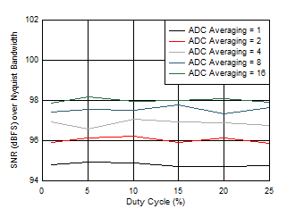
At 25°C, TX_SUP = 4 V, RX_SUP = IO_SUP = 3.3 V, 100-Hz PRF, 25% duty cycle, Rf = 500 kΩ, Cf is adjusted to keep the TIA time constant at 1/10th of the sampling duration, 8-MHz external clock (with CLKDIV_EXTMODE set to divide-by-2), CLKDIV_PRF = 1, detector CIN = 50 pF, ADC averaging = max allowed, SNR (dBFS) = noise referred to full-scale range of 2 V, noise integrated from 1 Hz to Nyquist (= PRF / 2), and values assigned to CLKDIV_EXTMODE and CLK_DIV_PRF parameters correspond to division ratios controlled by these modes, unless otherwise specified.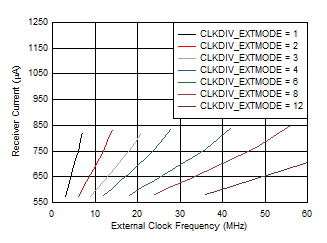
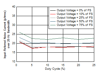
| Duty cycle (x-axis) refers to the sampling duration expressed as a percentage of the pulse repetition period. |
(As a Percentage of Full-Scale)
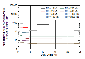
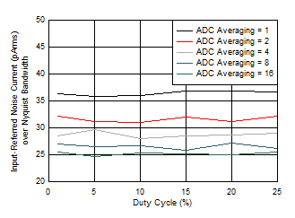
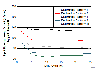 Figure 9. Input-Referred Noise Current in Nyquist Bandwidth vs Duty Cycle (Different Decimation Factor)
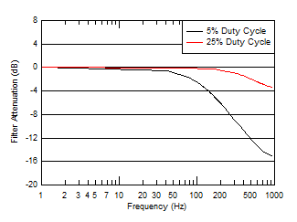
| PRF = 2000 Hz |
at the AFE Output
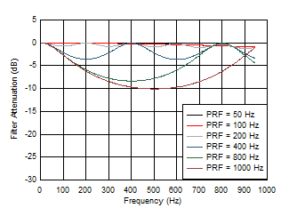
5% Duty Cycle
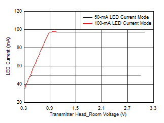
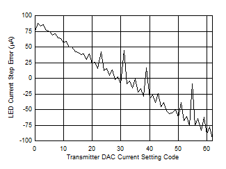
100-mA Mode
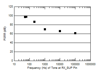
| Duty cycle = 1% |
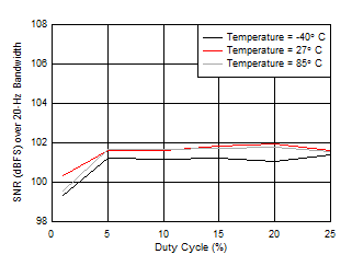
Duty Cycle Across Different Temperatures
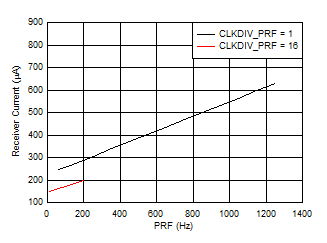
| Active window = 500 µs, LED pulse = 100 µs, all four DYNAMIC bits set to 1 |
Dynamic Power-Down Mode
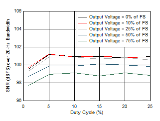
| Duty cycle (x-axis) refers to the sampling duration expressed as a percentage of the pulse repetition period. |
(As a Percentage of Full-Scale)
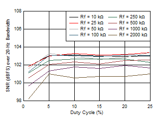
(Different TIA Gain Settings)
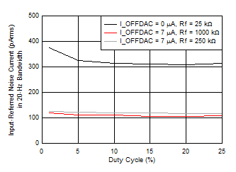
(Different Offset Cancellation DAC Currents)
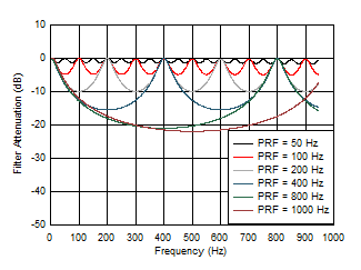
1% Duty Cycle
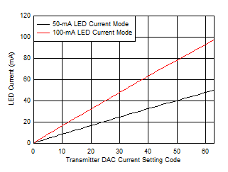
50-mA Mode
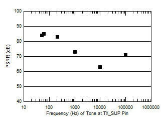
| Duty cycle = 1% |
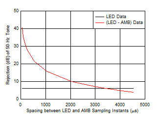
| PRF = 200 Hz, NUMAV = 0 |
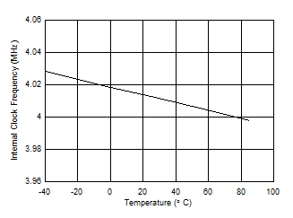
Temperature on a Typical Unit