ZHCSGX5 October 2017 ADS54J64
PRODUCTION DATA.
- 1 特性
- 2 应用
- 3 说明
- 4 修订历史记录
- 5 Pin Configuration and Functions
-
6 Specifications
- 6.1 Absolute Maximum Ratings
- 6.2 ESD Ratings
- 6.3 Recommended Operating Conditions
- 6.4 Thermal Information
- 6.5 Electrical Characteristics
- 6.6 AC Performance
- 6.7 Digital Characteristics
- 6.8 Timing Characteristics
- 6.9 Typical Characteristics: DDC Bypass Mode
- 6.10 Typical Characteristics: Mode 2
- 6.11 Typical Characteristics: Mode 0
- 6.12 Typical Characteristics: Dual ADC Mode
-
7 Detailed Description
- 7.1 Overview
- 7.2 Functional Block Diagram
- 7.3 Feature Description
- 7.4
Device Functional Modes
- 7.4.1
Digital Functions
- 7.4.1.1 Numerically Controlled Oscillators (NCOs) and Mixers
- 7.4.1.2 Decimation Filter
- 7.4.1.3 Mode 0: Decimate-by-4 With IQ Outputs and fS / 4 Mixer
- 7.4.1.4 Mode 1: Decimate-by-4 With IQ Outputs and 16-Bit NCO
- 7.4.1.5 Mode 2: Decimate-by-4 With Real Output
- 7.4.1.6 Mode 3: Decimate-by-2 Real Output With Frequency Shift
- 7.4.1.7 Mode 4: Decimate-by-4 With Real Output
- 7.4.1.8 Mode 6: Decimate-by-4 With IQ Outputs for Up to 110 MHz of IQ Bandwidth
- 7.4.1.9 Mode 7: Decimate-by-4 With Real Output and Zero Stuffing
- 7.4.1.10 Mode 8: DDC Bypass Mode
- 7.4.1.11 Averaging Mode
- 7.4.1.12 Overrange Indication
- 7.4.1
Digital Functions
- 7.5 Programming
- 7.6
Register Maps
- 7.6.1
Register Map
- 7.6.1.1
Register Description
- 7.6.1.1.1
GLOBAL Page Register Description
- 7.6.1.1.1.1 Register 00h (address = 00h) [reset = 0h], GLOBAL Page
- 7.6.1.1.1.2 Register 04h (address = 04h) [reset = 0h], GLOBAL Page
- 7.6.1.1.1.3 Register 11h (address = 11h) [reset = 0h], GLOBAL Page
- 7.6.1.1.1.4 Register 12h (address = 12h) [reset = 0h], GLOBAL Page
- 7.6.1.1.1.5 Register 13h (address = 13h) [reset = 0h], GLOBAL Page
- 7.6.1.1.2
DIGTOP Page Register Description
- 7.6.1.1.2.1 Register 64h (address = 64h) [reset = 0h], DIGTOP Page
- 7.6.1.1.2.2 Register 8Dh (address = 8Dh) [reset = 0h], DIGTOP Page
- 7.6.1.1.2.3 Register 8Eh (address = 8Eh) [reset = 0h], DIGTOP Page
- 7.6.1.1.2.4 Register 8Fh (address = 8Fh) [reset = 0h], DIGTOP Page
- 7.6.1.1.2.5 Register 90h (address = 90h) [reset = 0h], DIGTOP Page
- 7.6.1.1.2.6 Register 91h (address = 91h) [reset = 0h], DIGTOP Page
- 7.6.1.1.2.7 Register A5h (address = A5h) [reset = 0h], DIGTOP Page
- 7.6.1.1.2.8 Register A6h (address = A6h) [reset = 0h], DIGTOP Page
- 7.6.1.1.2.9 Register ABh (address = ABh) [reset = 0h], DIGTOP Page
- 7.6.1.1.2.10 Register ACh (address = ACh) [reset = 0h], DIGTOP Page
- 7.6.1.1.2.11 Register ADh (address = ADh) [reset = 0h], DIGTOP Page
- 7.6.1.1.2.12 Register AEh (address = AEh) [reset = 0h], DIGTOP Page
- 7.6.1.1.2.13 Register B7h (address = B7h) [reset = 0h], DIGTOP Page
- 7.6.1.1.2.14 Register 8Ch (address = 8Ch) [reset = 0h], DIGTOP Page
- 7.6.1.1.3
ANALOG Page Register Description
- 7.6.1.1.3.1 Register 6Ah (address = 6Ah) [reset = 0h], ANALOG Page
- 7.6.1.1.3.2 Register 6Fh (address = 6Fh) [reset = 0h], ANALOG Page
- 7.6.1.1.3.3 Register 71h (address = 71h) [reset = 0h], ANALOG Page
- 7.6.1.1.3.4 Register 72h (address = 72h) [reset = 0h], ANALOG Page
- 7.6.1.1.3.5 Register 93h (address = 93h) [reset = 0h], ANALOG Page
- 7.6.1.1.3.6 Register 94h (address = 94h) [reset = 0h], ANALOG Page
- 7.6.1.1.3.7 Register 9Bh (address = 9Bh) [reset = 0h], ANALOG Page
- 7.6.1.1.3.8 Register 9Dh (address = 9Dh) [reset = 0h], ANALOG Page
- 7.6.1.1.3.9 Register 9Eh (address = 9Eh) [reset = 0h], ANALOG Page
- 7.6.1.1.3.10 Register 9Fh (address = 9Fh) [reset = 0h], ANALOG Page
- 7.6.1.1.3.11 Register AFh (address = AFh) [reset = 0h], ANALOG Page
- 7.6.1.1.4
SERDES_XX Page Register Description
- 7.6.1.1.4.1 Register 20h (address = 20h) [reset = 0h], SERDES_XX Page
- 7.6.1.1.4.2 Register 21h (address = 21h) [reset = 0h], SERDES_XX Page
- 7.6.1.1.4.3 Register 22h (address = 22h) [reset = 0h], SERDES_XX Page
- 7.6.1.1.4.4 Register 23h (address = 23h) [reset = 0h], SERDES_XX Page
- 7.6.1.1.4.5 Register 25h (address = 25h) [reset = 0h], SERDES_XX Page
- 7.6.1.1.4.6 Register 26h (address = 26h) [reset = 0h], SERDES_XX Page
- 7.6.1.1.4.7 Register 28h (address = 28h) [reset = 0h], SERDES_XX Page
- 7.6.1.1.4.8 Register 2Dh (address = 2Dh) [reset = 0h], SERDES_XX Page
- 7.6.1.1.4.9 Register 36h (address = 36h) [reset = 0h], SERDES_XX Page
- 7.6.1.1.4.10 Register 41h (address = 41h) [reset = 0h], SERDES_XX Page
- 7.6.1.1.4.11 Register 42h (address = 42h) [reset = 0h], SERDES_XX Page
- 7.6.1.1.5
CHX Page Register Description
- 7.6.1.1.5.1 Register 26h (address = 26h) [reset = 0h], CHX Page
- 7.6.1.1.5.2 Register 27h (address = 27h) [reset = 0h], CHX Page
- 7.6.1.1.5.3 Register 2Dh (address = 2Dh) [reset = 0h], CHX Page
- 7.6.1.1.5.4 Register 78h (address = 78h) [reset = 0h], CHX Page
- 7.6.1.1.5.5 Register 7Ah (address = 7Ah) [reset = 0h], CHX Page
- 7.6.1.1.5.6 Register 7Bh (address = 7Bh) [reset = 0h], CHX Page
- 7.6.1.1.5.7 Register 7Eh (address = 7Eh) [reset = 3h], CHX Page
- 7.6.1.1.6
ADCXX Page Register Description
- 7.6.1.1.6.1 Register 07h (address = 07h) [reset = FFh], ADCXX Page
- 7.6.1.1.6.2 Register 08h (address = 08h) [reset = 0h], ADCXX Page
- 7.6.1.1.6.3 Register D5h (address = D5h) [reset = 0h], ADCXX Page
- 7.6.1.1.6.4 Register 2Ah (address = 2Ah) [reset = 0h], ADCXX Page
- 7.6.1.1.6.5 Register CFh (address = CFh) [reset = 0h], ADCXX Page
- 7.6.1.1.1
GLOBAL Page Register Description
- 7.6.1.1
Register Description
- 7.6.1
Register Map
- 8 Application and Implementation
- 9 Power Supply Recommendations
- 10Layout
- 11器件和文档支持
- 12机械、封装和可订购信息
7 Detailed Description
7.1 Overview
The ADS54J64 is a quad-channel device with a complex digital down-converter (DDC) and digital decimation to allow flexible signal processing to suit different usage cases. Each channel is composed of two interleaved analog-to-digital converters (ADCs) sampling at half the input clock rate. The 2x interleaved data are decimated by 2 to provide a processing gain of 3 dB. The decimation filter has a programmable option to be configured as low pass (default) or high pass. In default mode, the device operates in DDC mode 0, where the input is mixed with a constant frequency of –fS / 4 and transmitted as complex IQ. In DDC bypass mode (mode 8), the DDC is bypassed and the 2x decimated data are available on the JESD output. The different operational modes of the ADS54J64 are listed in Table 1.
The ADS54J64 can also be operated in a dual-channel interleaved mode (dual mode), in which two channels are averaged and the 2x interleaved and averaged data are available directly at the JESD output.
7.2 Functional Block Diagram
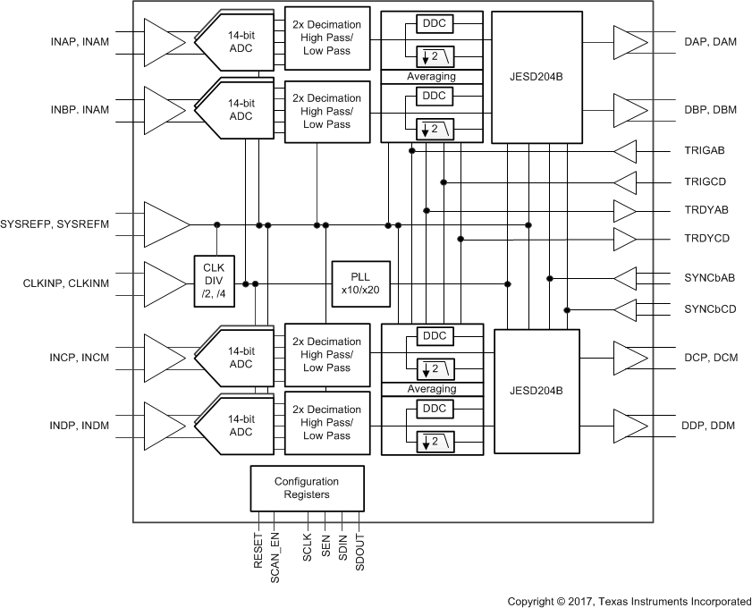
7.3 Feature Description
7.3.1 Analog Inputs
The ADS54J64 analog signal inputs are designed to be driven differentially. The analog input pins have internal analog buffers that drive the sampling circuit. As a result of the analog buffer, the input pins present a high-impedance input across a very wide frequency range to the external driving source that enables great flexibility in the external analog filter design as well as excellent 50-Ω matching for RF applications. The buffer also helps isolate the external driving circuit from the internal switching currents of the sampling circuit, resulting in a more constant SFDR performance across input frequencies. The common-mode voltage of the signal inputs is internally biased to 1.3 V using 2-kΩ resistors to allow for ac-coupling of the input drive network. Each input pin (INP, INM) must swing symmetrically between (VCM + 0.275 V) and (VCM – 0.275 V), resulting in a 1.1-VPP (default) differential input swing. The input sampling circuit has a 3-dB bandwidth that extends up to 1000 MHz.
7.3.2 Recommended Input Circuit
In order to achieve optimum ac performance, the following circuitry (shown in Figure 46) is recommended at the analog inputs.
 Figure 46. Analog Input Driving Circuit
7.3.3 Clock Input
The clock inputs of the ADS54J64 supports LVDS and LVPECL standards. The CLKP, CLKM inputs have an internal termination of 100 Ω. The clock inputs must be ac-coupled, as shown in Figure 47 and Figure 48, because the input pins are self-biased to a common-mode voltage of 0.7 V.
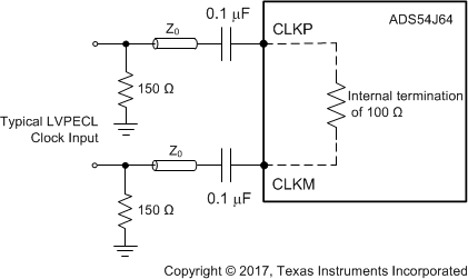 Figure 47. LVPECL Clock Driving Circuit
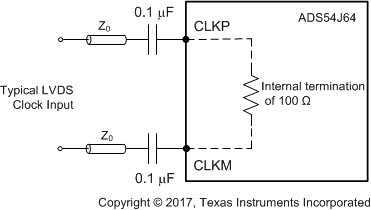 Figure 48. LVDS Clock Driving Circuit
7.4 Device Functional Modes
7.4.1 Digital Functions
Figure 49 shows the various operational modes available in the ADS54J64. In quad mode, the maximum output rate is half the sampling rate. The 2x interleaved data are filtered using a half-band filter (HBF) that can be configured as a low-pass or high-pass filter using register writes. In dual mode, the device can be operated at a full sampling rate with 2x interleaving and averaging of two channels.
Quad mode supports a maximum complex and a real bandwidth of 200 MHz. The HBF output can be brought directly on the JESD lines at half rate. The complex data are obtained through a digital down-converter (DDC) that is comprised of a 16-bit numerically controlled oscillator (NCO) and a 100-MHz or 200-MHz filter. The DDC also has a real output mode where the data are decimated by 2 and mixed to fOUT / 4 to support a bandwidth of 100 MHz. In addition to the DDC modes, the HBF output can be decimated by 2 to obtain an overall decimation by 4 on the 2x interleaved data.
Dual mode supports a maximum sampling rate of 1 GSPS. The 2x interleaved data from channel A and channel B (and likewise channels C and D) can be averaged and given on the JESD lanes.
Table 1 lists all modes of operation with the maximum bandwidth provided at a sample rate of 491.52 MSPS and 368.64 MSPS.
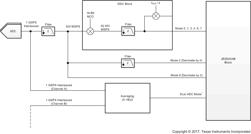
Table 1. ADS54J64 Operating Modes
| OPERATING MODE |
DESCRIPTION | 1ST-STAGE DECIMATION | DIGITAL MIXER |
2ND-STAGE DECIMATION | BANDWIDTH AT 491.52 MSPS |
BANDWIDTH AT 368.64 MSPS | OUTPUT MIXER |
OUTPUT FORMAT |
MAX OUTPUT RATE |
|---|---|---|---|---|---|---|---|---|---|
| 0 | Decimation | 2 | ±fS / 4 | 2 | 200 MHz | 150 MHz | — | Complex | 250 MSPS |
| 1 | 2 | 16-bit NCO | 2 | 200 MHz | 150 MHz | — | Complex | 250 MSPS | |
| 2 | 2 | — | 2 | 100 MHz (LP, LP or HP, HP), 75 MHz (HP, LP or LP, HP) |
75 MHz, 56.25 MHz |
— | Real | 250 MSPS | |
| 3 | 2 | 16-bit NCO | Bypass | 200 MHz | 150 MHz | fOUT / 4 | Real | 500 MSPS | |
| 4 | 2 | 16-bit NCO | 2 | 100 MHz | 75 MHz | fOUT / 4 | Real | 250 MSPS | |
| 5 | Reserved | Reserved | Reserved | Reserved | Reserved | Reserved | Reserved | Reserved | |
| 6 | 2 | 16-bit NCO | 4 | 100 MHz | 75 MHz | — | Complex | 125 MSPS | |
| 7 | 2 | 16-bit NCO | 2 | 100 MHz | 75 MHz | fOUT / 4 | Real with zero insertion | 500 MSPS | |
| 8 | DDC bypass mode | 2 | — | — | 223 MHz | 167 MHz | — | Real | 500 MSPS |
| 8 | Dual ADC mode | — | — | — | — | — | — | — | 1000 MSPS |
7.4.1.1 Numerically Controlled Oscillators (NCOs) and Mixers
The ADS54J64 is equipped with a complex numerically-controlled oscillator. The oscillator generates a complex exponential sequence: x[n] = ejωn. The frequency (ω) is specified by the 16-bit register setting. The complex exponential sequence is multiplied by the real input from the ADC to mix the desired carrier down to 0 Hz.
The NCO frequency setting is set by the 16-bit register value, NCO_FREQ[n]:

7.4.1.2 Decimation Filter
The ADS54J64 has two decimation filters (decimate-by-2) in the data path. The first stage of the decimation filter is non-programmable and is used in all functional modes. The second stage of decimation, available in DDC mode 2 and 6, can be used to obtain noise and linearity improvement for low bandwidth applications.
7.4.1.2.1 Stage-1 Filter
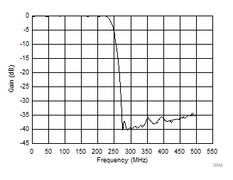
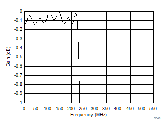
The first-stage filter is used for decimation of the 2x interleaved data from fCLK to fCLK / 2. Figure 50 and Figure 51 show the frequency response and pass-band ripple of the first-stage decimation filter, respectively.
| Input clock rate = 1 GHz |
| Input clock rate = 1 GHz |
7.4.1.2.2 Stage-2 Filter
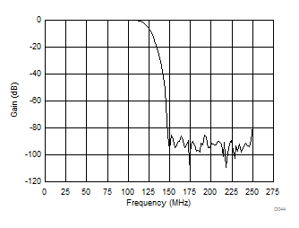
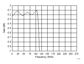
The second-stage filter is used for decimating the data from a sample rate of fCLK / 2 to fCLK / 4. Figure 52 and Figure 53 show the frequency response and pass-band ripple of the second-stage filter, respectively.
| Input clock rate (fCLK) = 1 GHz |
| Input clock rate (fCLK) = 1 GHz |
7.4.1.3 Mode 0: Decimate-by-4 With IQ Outputs and fS / 4 Mixer
In mode 0, the DDC block includes a fixed frequency ±fS / 4 complex digital mixer preceding the second-stage decimation filters. Figure 54 shows that the IQ pass band is approximately ±100 MHz centered at fS / 8 or 3fS / 8.
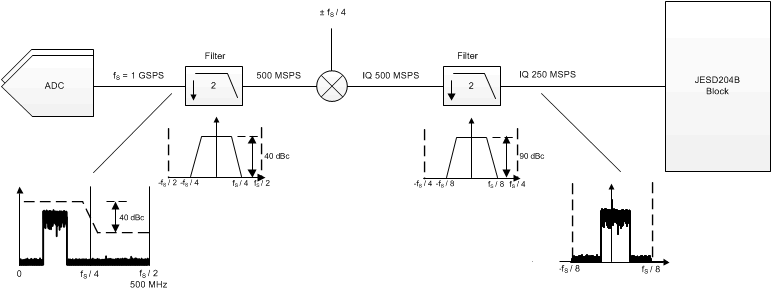 Figure 54. Operating Mode 0
7.4.1.4 Mode 1: Decimate-by-4 With IQ Outputs and 16-Bit NCO
In mode 1, the DDC block includes a 16-bit frequency resolution complex digital mixer, as shown in Figure 55, preceding the second-stage decimation filters.
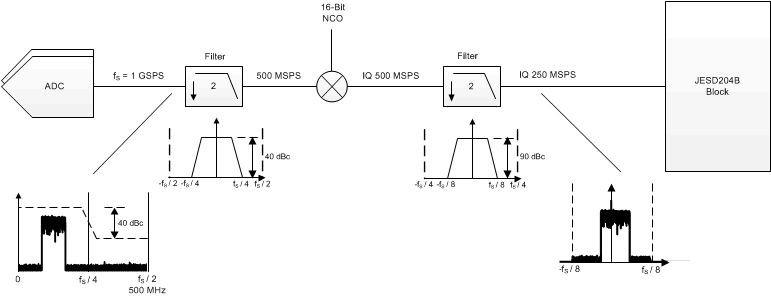 Figure 55. Operating Mode 1
7.4.1.5 Mode 2: Decimate-by-4 With Real Output
In mode 2, the DDC block cascades two decimate-by-2 filters. Each filter can be configured as low pass (LP) or high pass (HP), as shown in Table 2, to allow down conversion of different frequency ranges. Figure 56 shows that the LP, HP and HP, LP output spectra are inverted.
 Figure 56. Operating in Mode 2
Table 2. ADS54J64 Operating Mode 2, Down-Converted Frequency Ranges
| 1ST-STAGE FILTER | 2ND-STAGE FILTER | FREQUENCY RANGE WITH CLOCK RATE OF 983.04 MHz | BANDWIDTH WITH CLOCK RATE OF 983.04 MHz | FREQUENCY RANGE WITH CLOCK RATE OF 737.28 MHz | BANDWIDTH WITH CLOCK RATE OF 737.28 MHz |
|---|---|---|---|---|---|
| LP | LP | 0 MHz–100 MHz | 100 MHz | 0 MHz–75 MHz | 75 MHz |
| LP | HP | 150 MHz–223 MHz | 73 MHz | 112.5 MHz–167.25 MHz | 54.75 MHz |
| HP | LP | 268.52 MHz–341.52 MHz | 73 MHz | 201.39 MHz–256.14 MHz | 54.75 MHz |
| HP | HP | 391.52 MHz–491.52 MHz | 100 MHz | 293.64 MHz–368.64 MHz | 75 MHz |
7.4.1.6 Mode 3: Decimate-by-2 Real Output With Frequency Shift
In mode 3, the DDC block includes a 16-bit complex NCO digital mixer followed by a fS / 4 mixer with a real output to center the band at fS / 4. As shown in Figure 57, the NCO must be set to a value different from ±fS / 4, or else the samples are zeroed.
 Figure 57. Operating Mode 3
7.4.1.7 Mode 4: Decimate-by-4 With Real Output
In mode 4, the DDC block includes a 16-bit complex NCO digital mixer preceding the second-stage decimation filter. As shown in Figure 58, the signal is then mixed with fOUT / 4 to generate a real output. The bandwidth available in this mode is 100 MHz.
 Figure 58. Operating Mode 4
7.4.1.8 Mode 6: Decimate-by-4 With IQ Outputs for Up to 110 MHz of IQ Bandwidth
In mode 6, the DDC block shown in Figure 59 includes a 16-bit complex NCO digital mixer preceding a second-stage filter with a decimate-by-4 complex, generating a complex output at fS / 8.
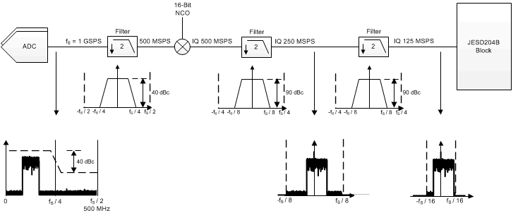 Figure 59. Operating Mode 6
7.4.1.9 Mode 7: Decimate-by-4 With Real Output and Zero Stuffing
In mode 7, the DDC block includes a 16-bit complex NCO digital mixer preceding the second-stage decimation filter. The signal is then mixed with fOUT / 4, as shown in Figure 60, to generate a real output that is then doubled in sample rate by zero-stuffing every other sample. The bandwidth available in this mode is 100 MHz.
 Figure 60. Operating Mode 7
7.4.1.10 Mode 8: DDC Bypass Mode
In mode 8, the DDC block is bypassed as shown in Figure 61 and the 2x decimated data are available on the JESD output. The decimation filter can be configured to be high pass or low pass using an SPI register bit. The stop-band attenuation is approximately 40 dB and the available bandwidth is 225 MHz. The decimation filter response is illustrated in Figure 50 and Figure 51.
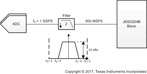 Figure 61. Operating Mode 8
7.4.1.11 Averaging Mode
In dual ADC mode, two channels (channels A, B and C, D) are averaged and given out as a single output. As a result, the device operates in a dual-channel mode with 2x interleaved sample rate. For a 1-GSPS input clock, the averaged output at 1 GSPS is available on two JESD lanes, each operating at 10 Gbps. Figure 62 shows the device supporting an averaging of channels A and B. An identical averaging path is available for channels C and D. Configure the device in mode 8 before enabling dual ADC mode through SPI register writes.
 Figure 62. Averaging Mode for Channels A and B (C and D Averaging is Identical)
7.4.1.12 Overrange Indication
The ADS54J64 provides a fast overrange indication that can be presented in the digital output data stream via SPI configuration. When the FOVR indication is embedded in the output data stream as shown in Figure 63, this indication replaces the LSB (D0) of the 16 bits going to the 8b, 10b encode.
 Figure 63. FOVR Timing Diagram
The fast overrange feature of the ADS54J64 is configured using an upper (FOVR Hi) and a lower (FOVR Lo) 8-bit threshold that are compared against the partial ADC output of the initial pipeline stages. Figure 64 shows the FOVR high and FOVR low thresholds.
The two thresholds are configured via the SPI register where a setting of 136 maps to the maximum ADC code for a high FOVR, and a setting of 8 maps to the minimum ADC code for a low FOVR.
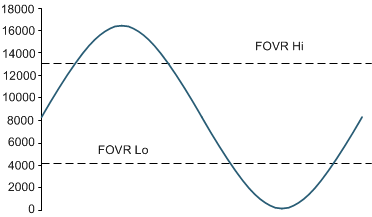 Figure 64. FOVR High and FOVR Low Thresholds
Equation 2 calculates the FOVR threshold from a full-scale input based on the ADC code:

Therefore, a threshold of –0.5 dBFS from full-scale can be set with:
- FOVR high = 132 (27h, 84h)
- FOVR low = 12 (28h, 0Ch)
7.5 Programming
7.5.1 JESD204B Interface
The ADS54J64 supports device subclass 1 with a maximum output data rate of 10 Gbps for each serial transmitter.
Figure 65 shows that an external SYSREF signal is used to align all internal clock phases and the local multi-frame clock to a specific sampling clock edge. A common SYSREF signal allows synchronization of multiple devices in a system and minimizes timing and alignment uncertainty. The ADS54J64 supports single (for all four JESD links) or dual (for channels A, B and C, D) SYNCb inputs and can be configured via the SPI.
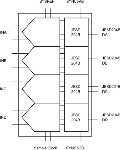 Figure 65. JESD204B Transmitter Block
Depending on the ADC sampling rate, the JESD204B output interface can be operated with one lane per channel. The JESD204B setup and configuration of the frame assembly parameters is handled via the SPI interface.
The JESD204B transmitter block shown in Figure 66 consists of the transport layer, the data scrambler, and the link layer. The transport layer maps the ADC output data into the selected JESD204B frame data format and manages if the ADC output data or test patterns are being transmitted. The link layer performs the 8b, 10b data encoding as well as the synchronization and initial lane alignment using the SYNC input signal. Optionally, data from the transport layer can be scrambled.
 Figure 66. JESD Interface Block Diagram
7.5.2 JESD204B Initial Lane Alignment (ILA)
The initial lane alignment process is started by the receiving device by deasserting the SYNCb signal. When a logic low is detected on the SYNC input pins, as shown in Figure 67, the ADS54J64 starts transmitting comma (K28.5) characters to establish code group synchronization.
When synchronization is complete, the receiving device reasserts the SYNCb signal and the ADS54J64 starts the initial lane alignment sequence with the next local multi-frame clock boundary. The ADS54J64 transmits four multi-frames, each containing K frames (K is SPI programmable). Each of the multi-frames contains the frame start and end symbols and the second multi-frame also contains the JESD204 link configuration data.
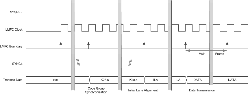 Figure 67. ILA Sequence
7.5.3 JESD204B Frame Assembly
The JESD204B standard defines the following parameters:
- L is the number of lanes per link
- M is the number of converters per device
- F is the number of octets per frame clock period
- S is the number of samples per frame
Table 3 lists the available JESD204B formats and valid ranges for the ADS54J64. The ranges are limited by the SerDes line rate and the maximum ADC sample frequency.
Table 3. Available JESD204B Formats and Valid Ranges for the ADS54J64
| L | M | F | S | OPERATING MODE | DIGITAL MODE | OUTPUT FORMAT | MAX ADC OUTPUT RATE (MSPS) |
MAX fSerDes
(Gbps) |
JESD PLL REGISTER CONFIGURATION |
|---|---|---|---|---|---|---|---|---|---|
| 4 | 8 | 4 | 1 | 0, 1 | 2x decimation | Complex | 250 | 10.0 | — |
| 4 | 4 | 2 | 1 | 2, 4 | 2x decimation | Real | 250 | 5.0 | CTRL_SER_MODE = 1, SerDes_MODE = 1 |
| 2 | 4 | 4 | 1 | 2, 4 | 2x decimation | Real | 250 | 10.0 | — |
| 4 | 8 | 4 | 1 | 6 | 4x decimation | Complex | 125 | 5.0 | — |
| 2 | 8 | 8 | 1 | 6 | 4x decimation | Complex | 125 | 10.0 | CTRL_SER_MODE = 1, SerDes_MODE = 3 |
| 4 | 4 | 2 | 1 | 7 | 2x decimation with 0-pad | Real | 500 | 10.0 | — |
| 4 | 4 | 2 | 1 | 3, 8 | DDC bypass | Real | 500 | 10.0 | — |
| 4 | 2 | 1 | 1 | 8 | DDC bypass dual ADC | Real | 1000 | 10.0 | — |
Table 4, Table 5, and Table 6 show the detailed frame assembly for various LMFS settings.
Table 4. Detailed Frame Assembly for Four-Lane Modes (Modes 0, 1, 3, 6, 7, and 8)
| OUTPUT LANE | LMFS = 4841 | LMFS = 4421 | LMFS = 4421 | |||||||||
|---|---|---|---|---|---|---|---|---|---|---|---|---|
| DA | AI0[15:8] | AI0[7:0] | AQ0[15:8] | AQ0[7:0] | A0[15:8] | A0[7:0] | A1[15:8] | A1[7:0] | A0[15:8] | A0[7:0] | 0000 0000 | 0000 0000 |
| DB | BI0[15:8] | BI0[7:0] | BQ0[15:8] | BQ0[7:0] | B0[15:8] | B0[7:0] | B1[15:8] | B1[7:0] | B0[15:8] | B0[7:0] | 0000 0000 | 0000 0000 |
| DC | CI0[15:8] | CI0[7:0] | CQ0[15:8] | CQ0[7:0] | C0[15:8] | C0[7:0] | C1[15:8] | C1[7:0] | C0[15:8] | C0[7:0] | 0000 0000 | 0000 0000 |
| DD | DI0[15:8] | DI0[7:0] | DQ0[15:8] | DQ0[7:0] | D0[15:8] | D0[7:0] | D1[15:8] | D1[7:0] | D0[15:8] | D0[7:0] | 0000 0000 | 0000 0000 |
Table 5. Detailed Frame Assembly for Two-Lane Modes (Modes 2 and 4)
| OUTPUT LANE | LMFS = 2441 | LMFS = 2881 | ||||||||||
|---|---|---|---|---|---|---|---|---|---|---|---|---|
| DB | A0[15:8] | A0[7:0] | B0[15:8] | B0[7:0] | AI0[15:8] | AI0[7:0] | AQ0[15:8] | AQ0[7:0] | BI0[15:8] | BI0[7:0] | BQ0[15:8] | BQ0[7:0] |
| DC | C0[15:8] | C0[7:0] | D0[15:8] | D0[7:0] | CI0[15:8] | CI0[7:0] | CQ0[15:8] | CQ0[7:0] | DI0[15:8] | DI0[7:0] | DQ0[15:8] | DQ0[7:0] |
Table 6. Detailed Frame Assembly for Four-Lane Mode (2x Interleaved Dual ADC)
| OUTPUT LANE | LMFS = 4211 | |||
|---|---|---|---|---|
| DA | AB(1)0[15:8] | AB1[15:8] | AB2[15:8] | AB3[15:8] |
| DB | AB0[7:0] | AB1[7:0] | AB2[7:0] | AB3[7:0] |
| DC | CD(2)0[15:8] | CD1[15:8] | CD2[15:8] | CD3[15:8] |
| DD | CD0[7:0] | CD1[7:0] | CD2[7:0] | CD3[7:0] |
7.5.4 JESD Output Switch
To ease layout constraints, the ADS54J64 provides a digital cross-point switch in the JESD204B block (as shown in Figure 68) that allows internal routing of any output of the two ADCs within one channel pair to any of the two JESD204B serial transmitters. The cross-point switch routing is configured via the SPI (address 41h in the SERDES_XX digital page).
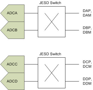 Figure 68. Switching the Output Lanes
7.5.4.1 SerDes Transmitter Interface
As shown in Figure 69, each 10-Gbps SerDes transmitter output requires ac-coupling between the transmitter and receiver. Terminate the differential pair with 100 Ω as close to the receiving device as possible to avoid unwanted reflections and signal degradation.
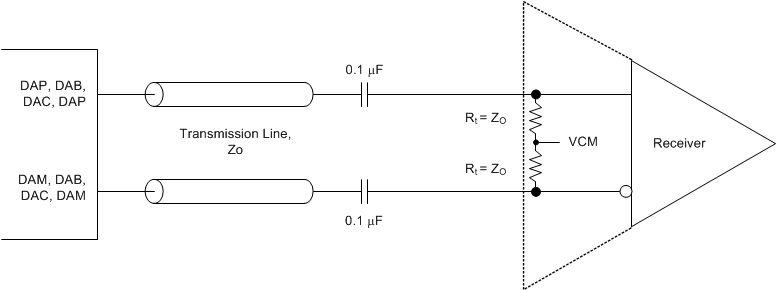 Figure 69. SerDes Transmitter Connection to Receiver
7.5.4.2 SYNCb Interface
The ADS54J64 supports single SYNCb control (where the SYNCb input controls all four JESD204B links) or dual SYNCb control (where one SYNCb input controls two JESD204B lanes: DA, DB and DC, DD). When using the single SYNCb control, connect the unused input to a differential logic high (SYNCbxxP = DVDD, SYNCbxxM = 0 V).
7.5.4.3 Eye Diagram
Figure 70 to Figure 73 show the serial output eye diagrams of the ADS54J64 at 7.5 Gbps and 10 Gbps with default and increased output voltage swing against the JESD204B mask.
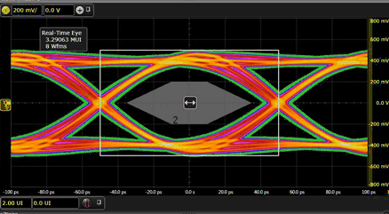 Figure 70. Eye at 10-Gbps Bit Rate With
 Default Output Swing
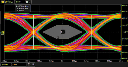 Figure 72. Eye at 10-Gbps Bit Rate With
 Increased Output Swing
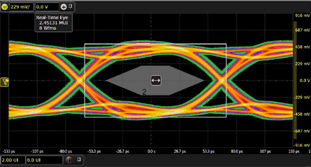 Figure 71. Eye at 7.5-Gbps Bit Rate With
 Default Output Swing
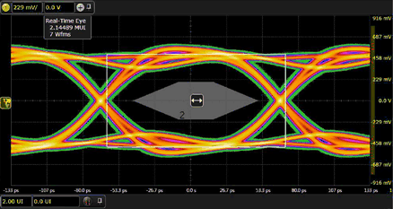 Figure 73. Eye at 7.5-Gbps Bit Rate With
 Increased Output Swing
7.5.5 Device Configuration
The ADS54J64 can be configured using a serial programming interface, as described in the Register Maps section. In addition, the device has one dedicated parallel pin (PDN) for controlling the power-down modes. The ADS54J64 supports a 24-bit (16-bit address, 8-bit data) SPI operation and uses paging to access all register bits.
7.5.5.1 Details of the Serial Interface
The ADC has a set of internal registers that can be accessed by the serial interface formed by the SEN (serial interface enable), SCLK (serial interface clock), SDIN (serial data input data), and SDOUT (serial data output) pins. Serially shifting bits into the device is enabled when SEN is low. SDIN serial data are latched at every SCLK rising edge when SEN is active (low). Data can be loaded in multiples of 24-bit words within a single active SEN pulse. The first 16 bits form the register address and the remaining eight bits are the register data. The interface can work with SCLK frequencies from 10 MHz down to very low speeds (of a few hertz) and also with a non-50% SCLK duty cycle.
7.5.5.1.1 Register Initialization
After power-up, the internal registers must be initialized to the default values. This initialization can be accomplished in one hardware reset by applying a high pulse on the RESET pin.
7.5.5.2 Serial Register Write
The internal registers of the ADS54J64 can be programmed (as shown in Figure 74) by:
- Driving the SEN pin low
- Setting the R/W bit = 0
- Initiating a serial interface cycle specifying the address of the register (A[14:0]) whose content must be written
- Writing the 8-bit data that is latched in on the SCLK rising edge
The ADS54J64 has several different register pages (page selection in address 11h, 12h). Specify the register page before writing to the desired address. The register page only must be set one time for continuous writes to the same page.
During the write operation, the SDOUT pin is in a high-impedance mode and must float.
 Figure 74. Serial Interface Write Timing Diagram
7.5.5.3 Serial Read
Figure 75 shows a typical 4-wire serial register readout. In the default 4-pin configuration, the SDIN pin is the data output from the ADS54J64 during the data transfer cycle when SDOUT is in a high-impedance state. The internal registers of the ADS54J64 can be read out by:
- Driving the SEN pin low
- Setting the R/W bit to 1 to enable read back
- Specifying the address of the register (A[14:0]) whose content must be read back
- The device outputs the contents (D[7:0]) of the selected register on the SDOUT pin (pin 51)
- The external controller can latch the contents at the SCLK rising edge
 Figure 75. Serial Interface 4-Wire Read Timing Diagram
7.6 Register Maps
7.6.1 Register Map
The ADS54J64 registers are organized on different pages depending on their internal functions. The pages are accessed by selecting the page in the master pages 11h–13h. The page selection must only be written one time for a continuous update of registers for that page.
There are six different SPI banks (see Figure 76 and Table 7) that group together different functions:
- GLOBAL: contains controls for accessing other SPI banks
- DIGTOP: top-level digital functions
- ANALOG: registers controlling power-down and analog functions
- SERDES_XX: registers controlling JESD204B functions
- CHX: registers controlling channel-specific functions, including DDC
- ADCXX: register page for one of the eight interleaved ADCs
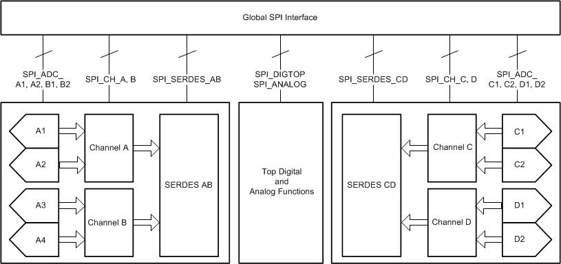 Figure 76. SPI Register Block Diagram
Table 7. Serial Interface Register Map
| ADDRESS (Hex) | 7 | 6 | 5 | 4 | 3 | 2 | 1 | 0 |
|---|---|---|---|---|---|---|---|---|
| GLOBAL PAGE | ||||||||
| 00h | WRITE_1 | 0 | 0 | 0 | 0 | 0 | 0 | SW_RESET |
| 04h | VERSION_ID | |||||||
| 11h | SPI_D2 | SPI_D1 | SPI_C2 | SPI_C1 | SPI_B2 | SPI_B1 | SPI_A2 | SPI_A1 |
| 12h | 0 | SPI_SERDES_CD | SPI_SERDES_AB | SPI_CHD | SPI_CHC | SPI_CHB | SPI_CHA | SPI_DIGTOP |
| 13h | 0 | 0 | 0 | 0 | 0 | 0 | 0 | SPI_ANALOG |
| DIGTOP PAGE | ||||||||
| 64h | 0 | 0 | 0 | 0 | 0 | 0 | FS_375_500 | 0 |
| 8Dh | CUSTOMPATTERN1[7:0] | |||||||
| 8Eh | CUSTOMPATTERN1[15:8] | |||||||
| 8Fh | CUSTOMPATTERN2[7:0] | |||||||
| 90h | CUSTOMPATTERN2[15:8] | |||||||
| 91h | TESTPATTERNSELECT | TESTPATTERNENCHD | TESTPATTERNENCHC | TESTPATTERNENCHB | TESTPATTERNENCHA | |||
| A5h | 0 | 0 | 0 | 0 | 0 | 0 | CH_CD_AVG_EN | CH_AB_AVG_EN |
| A6h | 0 | 0 | AVG_ENABLE | OVR_ON_LSB | GAIN_WORD_ENABLE | 0 | 0 | 0 |
| ABh | 0 | 0 | 0 | 0 | 0 | 0 | INTERLEAVE_A | SPECIALMODE0 |
| ACh | 0 | 0 | 0 | 0 | 0 | 0 | INTERLEAVE_C | SPECIALMODE1 |
| ADh | 0 | 0 | 0 | 0 | DDCMODEAB | |||
| AEh | 0 | 0 | 0 | 0 | DDCMODECD | |||
| B7h | 0 | 0 | 0 | 0 | 0 | 0 | 0 | LOAD_TRIMS |
| 8Ch | 0 | 0 | 0 | 0 | 0 | 0 | ENABLE_LOAD_TRIMS | 0 |
| ANALOG PAGE | ||||||||
| 6Ah | 0 | 0 | 0 | 0 | 0 | 0 | DIS_SYSREF | 0 |
| 6Fh | 0 | JESD_SWING | 0 | 0 | 0 | 0 | ||
| 71h | EMP_LANE_B[5:4] | EMP_LANE_A | ||||||
| 72h | 0 | 0 | 0 | 0 | EMP_LANE_B[3:0] | |||
| 93h | EMP_LANE_D[5:4] | EMP_LANE_C | ||||||
| 94h | 0 | 0 | 0 | 0 | EMP_LANE_D[3:0] | |||
| 9Bh | 0 | 0 | 0 | SYSREF_PDN | 0 | 0 | 0 | 0 |
| 9Dh | PDN_CHA | PDN_CHB | 0 | 0 | PDN_CHD | PDN_CHC | 0 | 0 |
| 9Eh | 0 | 0 | 0 | PDN_SYNCAB | 0 | 0 | 0 | PDN_GLOBAL |
| 9Fh | 0 | 0 | 0 | 0 | 0 | 0 | PIN_PDN_MODE | FAST_PDN |
| AFh | 0 | 0 | 0 | 0 | 0 | 0 | PDN_SYNCCD | 0 |
| SERDES_XX PAGE | ||||||||
| 20h | CTRL_K | CTRL_SER_MODE | 0 | TRANS_TEST_EN | 0 | LANE_ALIGN | FRAME_ALIGN | TX_ILA_DIS |
| 21h | SYNC_REQ | OPT_SYNC_REQ | SYNCB_SEL_AB_CD | 0 | 0 | 0 | SERDES_MODE | |
| 22h | LINK_LAYER_TESTMODE_SEL | RPAT_SET_DISP | LMFC_MASK_RESET | 0 | 0 | 0 | ||
| 23h | FORCE_LMFC_COUNT | LMFC_CNT_INIT | RELEASE_ILANE_REQ | |||||
| 25h | SCR_EN | 0 | 0 | 0 | 0 | 0 | 0 | 0 |
| 26h | 0 | 0 | 0 | K_NO_OF_FRAMES_PER_MULTIFRAME | ||||
| 28h | 0 | 0 | 0 | 0 | CTRL_LID | 0 | 0 | 0 |
| 2Dh | LID1 | LID2 | ||||||
| 36h | PRBS_MODE | 0 | 0 | 0 | 0 | 0 | 0 | |
| 41h | LANE_BONA | LANE_AONB | ||||||
| 42h | 0 | 0 | 0 | 0 | INVERT_AC | INVERT_BD | ||
| CHX PAGE | ||||||||
| 26h | 0 | 0 | 0 | 0 | 0 | 0 | GAINWORD | |
| 27h | OVR_ENABLE | OVR_FAST_SEL | 0 | 0 | OVR_LSB1 | 0 | OVR_LSB0 | 0 |
| 2Dh | 0 | 0 | 0 | 0 | 0 | 0 | NYQUIST_SELECT | 0 |
| 78h | 0 | 0 | 0 | 0 | 0 | FS4_SIGN | NYQ_SEL_MODE02 | NYQ_SEL |
| 7Ah | NCO_WORD[15:8] | |||||||
| 7Bh | NCO_WORD[7:0] | |||||||
| 7Eh | 0 | 0 | 0 | 0 | 0 | MODE467_GAIN | MODE0_GAIN | MODE13_GAIN |
| ADCXX PAGE | ||||||||
| 07h | FAST_OVR_THRESHOLD_HIGH | |||||||
| 08h | FAST_OVR_THRESHOLD_LOW | |||||||
| D5h | 0 | 0 | 0 | 0 | CAL_EN | 0 | 0 | 0 |
| 2Ah | 0 | 0 | 0 | 0 | 0 | 0 | 0 | ADC_TRIM1 |
| CFh | ADC_TRIM2 | 0 | 0 | 0 | 0 | |||
7.6.1.1 Register Description
Table 8 lists the access codes for the ADS54J64 registers.
Table 8. ADS54J64 Access Type Codes
| Access Type | Code | Description |
|---|---|---|
| R | R | Read |
| R/W | R-W | Read or Write |
| W | W | Write |
| -n | Value after reset or the default value |
7.6.1.1.1 GLOBAL Page Register Description
7.6.1.1.1.1 Register 00h (address = 00h) [reset = 0h], GLOBAL Page
| 7 | 6 | 5 | 4 | 3 | 2 | 1 | 0 |
| WRITE_1 | 0 | 0 | 0 | 0 | 0 | 0 | SW_RESET |
| R/W-0h | R/W-0h | R/W-0h | R/W-0h | R/W-0h | R/W-0h | R/W-0h | R/W-0h |
Table 9. Register 00h Field Descriptions
| Bit | Field | Type | Reset | Description |
|---|---|---|---|---|
| 7 | WRITE_1 | R/W | 0h | Always write 1 |
| 6-1 | 0 | R/W | 0h | Must read or write 0 |
| 0 | SW_RESET | R/W | 0h | This bit rests the device. |
7.6.1.1.1.2 Register 04h (address = 04h) [reset = 0h], GLOBAL Page
| 7 | 6 | 5 | 4 | 3 | 2 | 1 | 0 |
| VERSION_ID | |||||||
| R-0h | |||||||
Table 10. Register 04h Field Descriptions
| Bit | Field | Type | Reset | Description |
|---|---|---|---|---|
| 7-0 | VERSION_ID | R | 0h | These bits set the version ID of the device. 16 : PG 1.0 32 : PG 2.0 48 : PG 3.0 |
7.6.1.1.1.3 Register 11h (address = 11h) [reset = 0h], GLOBAL Page
| 7 | 6 | 5 | 4 | 3 | 2 | 1 | 0 |
| SPI_D2 | SPI_D1 | SPI_C2 | SPI_C1 | SPI_B2 | SPI_B1 | SPI_A2 | SPI_A1 |
| R/W-0h | R/W-0h | R/W-0h | R/W-0h | R/W-0h | R/W-0h | R/W-0h | R/W-0h |
Table 11. Register 11h Field Descriptions
| Bit | Field | Type | Reset | Description |
|---|---|---|---|---|
| 7 | SPI_D2 | R/W | 0h | This bit selects the ADC D2 SPI. 0 : ADC D2 SPI is disabled 1 : ADC D2 SPI is enabled |
| 6 | SPI_D1 | R/W | 0h | This bit selects the ADC D1 SPI. 0 : ADC D1 SPI is disabled 1 : ADC D1 SPI is enabled |
| 5 | SPI_C2 | R/W | 0h | This bit selects the ADC C2 SPI 0 : ADC C2 SPI is disabled 1 : ADC C2 SPI is enabled |
| 4 | SPI_C1 | R/W | 0h | This bit selects the ADC C1 SPI. 0 : ADC C1 SPI is disabled 1 : ADC C1 SPI is enabled |
| 3 | SPI_B2 | R/W | 0h | This bit selects the ADC B2 SPI. 0 : ADC B2 SPI is disabled 1 : ADC B2 SPI is enabled |
| 2 | SPI_B1 | R/W | 0h | This bit selects the ADC B1 SPI. 0 : ADC B1 SPI is disabled 1 : ADC B1 SPI is enabled |
| 1 | SPI_A2 | R/W | 0h | This bit selects the ADC A2 SPI. 0 : ADC A2 SPI is disabled 1 : ADC A2 SPI is enabled |
| 0 | SPI_A1 | R/W | 0h | This bit selects the ADC A1 SPI. 0 : ADC A1 SPI is disabled 1 : ADC A1 SPI is enabled |
7.6.1.1.1.4 Register 12h (address = 12h) [reset = 0h], GLOBAL Page
| 7 | 6 | 5 | 4 | 3 | 2 | 1 | 0 |
| 0 | SPI_SERDES_CD | SPI_SERDES_AB | SPI_CHD | SPI_CHC | SPI_CHB | SPI_CHA | SPI_DIGTOP |
| R/W-0h | R/W-0h | R/W-0h | R/W-0h | R/W-0h | R/W-0h | R/W-0h | R/W-0h |
Table 12. Register 12h Field Descriptions
| Bit | Field | Type | Reset | Description |
|---|---|---|---|---|
| 7 | 0 | R/W | 0h | Must read or write 0 |
| 6 | SPI_SERDES_CD | R/W | 0h | This bit selects the channel CD SerDes SPI. 0 : Channel CD SerDes SPI is disabled 1 : Channel CD SerDes SPI is enabled |
| 5 | SPI_SERDES_AB | R/W | 0h | This bit selects the channel AB SerDes SPI. 0 : Channel AB SerDes is disabled 1 : Channel AB SerDes is enabled |
| 4 | SPI_CHD | R/W | 0h | This bit selects the channel D SPI. 0 : Channel D SPI is disabled 1 : Channel D SPI is enabled |
| 3 | SPI_CHC | R/W | 0h | This bit selects the channel C SPI. 0 : Channel C SPI is disabled 1 : Channel C SPI is enabled |
| 2 | SPI_CHB | R/W | 0h | This bit selects the channel B SPI. 0 : Channel B SPI is disabled 1 : Channel B SPI is enabled |
| 1 | SPI_CHA | R/W | 0h | This bit selects the channel A SPI. 0 : Channel A SPI is disabled 1 : Channel A SPI is enabled |
| 0 | SPI_DIGTOP | R/W | 0h | This bit selects the DIGTOP SPI. 0 : DIGTOP SPI is disabled 1 : DIGTOP SPI is enabled |
7.6.1.1.1.5 Register 13h (address = 13h) [reset = 0h], GLOBAL Page
| 7 | 6 | 5 | 4 | 3 | 2 | 1 | 0 |
| 0 | 0 | 0 | 0 | 0 | 0 | 0 | SPI_ANALOG |
| R/W-0h | R/W-0h | R/W-0h | R/W-0h | R/W-0h | R/W-0h | R/W-0h | R/W-0h |
Table 13. Register 13h Field Descriptions
| Bit | Field | Type | Reset | Description |
|---|---|---|---|---|
| 7-1 | 0 | R/W | 0h | Must read or write 0 |
| 0 | SPI_ANALOG | R/W | 0h | This bit selects the analog SPI. 0 : Analog SPI is disabled 1 : Analog SPI is enabled |
7.6.1.1.2 DIGTOP Page Register Description
7.6.1.1.2.1 Register 64h (address = 64h) [reset = 0h], DIGTOP Page
| 7 | 6 | 5 | 4 | 3 | 2 | 1 | 0 |
| 0 | 0 | 0 | 0 | 0 | 0 | FS_375_500 | 0 |
| R/W-0h | R/W-0h | R/W-0h | R/W-0h | R/W-0h | R/W-0h | R/W-0h | R/W-0h |
Table 14. Register 64h Field Descriptions
| Bit | Field | Type | Reset | Description |
|---|---|---|---|---|
| 7-2 | 0 | R/W | 0h | Must read or write 0 |
| 1 | FS_375_500 | R/W | 0h | This bit selects the clock rate for loading trims. 0 : 375 MSPS 1 : 500 MSPS |
| 0 | 0 | R/W | 0h | Must read or write 0 |
7.6.1.1.2.2 Register 8Dh (address = 8Dh) [reset = 0h], DIGTOP Page
| 7 | 6 | 5 | 4 | 3 | 2 | 1 | 0 |
| CUSTOMPATTERN1[7:0] | |||||||
| R/W-0h | |||||||
Table 15. Register 8Dh Field Descriptions
| Bit | Field | Type | Reset | Description |
|---|---|---|---|---|
| 7-0 | CUSTOMPATTERN1[7:0] | R/W | 0h | These bits set the custom pattern 1 that is used when the test pattern is enabled and set to a single or dual test pattern. |
7.6.1.1.2.3 Register 8Eh (address = 8Eh) [reset = 0h], DIGTOP Page
| 7 | 6 | 5 | 4 | 3 | 2 | 1 | 0 |
| CUSTOMPATTERN1[15:8] | |||||||
| R/W-0h | |||||||
Table 16. Register 8Eh Field Descriptions
| Bit | Field | Type | Reset | Description |
|---|---|---|---|---|
| 7-0 | CUSTOMPATTERN1[15:8] | R/W | 0h | These bits set the custom pattern 1 that is used when the test pattern is enabled and set to a single or dual test pattern. |
7.6.1.1.2.4 Register 8Fh (address = 8Fh) [reset = 0h], DIGTOP Page
| 7 | 6 | 5 | 4 | 3 | 2 | 1 | 0 |
| CUSTOMPATTERN2[7:0] | |||||||
| R/W-0h | |||||||
Table 17. Register 8Fh Field Descriptions
| Bit | Field | Type | Reset | Description |
|---|---|---|---|---|
| 7-0 | CUSTOMPATTERN2[7:0] | R/W | 0h | These bits set the custom pattern 2 that is used when the test pattern select is set to dual pattern mode. |
7.6.1.1.2.5 Register 90h (address = 90h) [reset = 0h], DIGTOP Page
| 7 | 6 | 5 | 4 | 3 | 2 | 1 | 0 |
| CUSTOMPATTERN2[15:8] | |||||||
| R/W-0h | |||||||
Table 18. Register 90h Field Descriptions
| Bit | Field | Type | Reset | Description |
|---|---|---|---|---|
| 7-0 | CUSTOMPATTERN2[15:8] | R/W | 0h | These bits set the custom pattern 2 that is used when the test pattern select is set to dual pattern mode. |
7.6.1.1.2.6 Register 91h (address = 91h) [reset = 0h], DIGTOP Page
| 7 | 6 | 5 | 4 | 3 | 2 | 1 | 0 |
| TESTPATTERNSELECT | TESTPATTERNENCHD | TESTPATTERNENCHC | TESTPATTERNENCHB | TESTPATTERNENCHA | |||
| R/W-0h | R/W-0h | R/W-0h | R/W-0h | R/W-0h | |||
Table 19. Register 91h Field Descriptions
| Bit | Field | Type | Reset | Description |
|---|---|---|---|---|
| 7-4 | TESTPATTERNSELECT | R/W | 0h | These bits select the test pattern on the output when the test pattern is enabled for a suitable channel. 0 : Default 1 : All zeros 2 : All ones 3 : Toggle pattern 4 : Ramp pattern 6 : Custom pattern 1 7 : Toggle between custom pattern 1 and custom pattern 2 8 : Deskew pattern (0xAAAA) |
| 3 | TESTPATTERNENCHD | R/W | 0h | This bit enables the channel D test pattern. 0 : Default data on channel D 1 : Enable test pattern on channel D |
| 2 | TESTPATTERNENCHC | R/W | 0h | This bit enables the channel C test pattern. 0 : Default data on channel C 1 : Enable test pattern on channel C |
| 1 | TESTPATTERNENCHB | R/W | 0h | This bit enables the channel B test pattern. 0 : Default data on channel B 1 : Enable test pattern on channel B |
| 0 | TESTPATTERNENCHA | R/W | 0h | This bit enables the channel A test pattern. 0 : Default data on channel A 1 : Enable test pattern on channel A |
7.6.1.1.2.7 Register A5h (address = A5h) [reset = 0h], DIGTOP Page
| 7 | 6 | 5 | 4 | 3 | 2 | 1 | 0 |
| 0 | 0 | 0 | 0 | 0 | 0 | CH_CD_AVG_EN | CH_AB_AVG_EN |
| R/W-0h | R/W-0h | R/W-0h | R/W-0h | R/W-0h | R/W-0h | R/W-0h | R/W-0h |
Table 20. Register A5h Field Descriptions
| Bit | Field | Type | Reset | Description |
|---|---|---|---|---|
| 7-2 | 0 | R/W | 0h | Must read or write 0 |
| 1 | CH_CD_AVG_EN | R/W | 0h | 0: Averaging is disabled for channels C, D 1: Averaging is enabled for channels C, D; set AVG_ENABLE in Register A6h (address = A6h) [reset = 0h], DIGTOP Page to 1 if using this option |
| 0 | CH_AB_AVG_EN | R/W | 0h | 0: Averaging is disabled for channels A, B 1: Averaging is enabled for channels A, B; set AVG_ENABLE in Register A6h (address = A6h) [reset = 0h], DIGTOP Page to 1 if using this option |
7.6.1.1.2.8 Register A6h (address = A6h) [reset = 0h], DIGTOP Page
| 7 | 6 | 5 | 4 | 3 | 2 | 1 | 0 |
| 0 | 0 | AVG_ENABLE | OVR_ON_ LSB |
GAIN_WORD_ ENABLE |
0 | 0 | 0 |
| R/W-0h | R/W-0h | R/W-0h | R/W-0h | R/W-0h | R/W-0h | R/W-0h | R/W-0h |
Table 21. Register A6h Field Descriptions
| Bit | Field | Type | Reset | Description |
|---|---|---|---|---|
| 7-6 | 0 | R/W | 0h | Must read or write 0 |
| 5 | AVG_ENABLE | R/W | 0h | 0: Default operation 1: Enable averaging option for the AB and CD channel pairs |
| 4 | OVR_ON_LSB | R/W | 0h | This bit enables the overrange indicator (OVR) on the LSB1 and LSB0 bits. OVR_LSB1 and OVR_LSB0 must be configured in register 27h of the CHX page. 0 : Default data 1 : OVR on LSB1 and LSB0 bits |
| 3 | GAIN_WORD_ENABLE | R/W | 0h | This bit enables the digital gain. Gain can be programmed using the GAINWORD bits in register 26h of the CHX page. 0 : Disable digital gain 1 : Enable digital gain |
| 2-0 | 0 | R/W | 0h | Must read or write 0 |
7.6.1.1.2.9 Register ABh (address = ABh) [reset = 0h], DIGTOP Page
| 7 | 6 | 5 | 4 | 3 | 2 | 1 | 0 |
| 0 | 0 | 0 | 0 | 0 | 0 | INTERLEAVE_A | SPECIALMODE0 |
| R/W-0h | R/W-0h | R/W-0h | R/W-0h | R/W-0h | R/W-0h | R/W-0h | R/W-0h |
Table 22. Register ABh Field Descriptions
| Bit | Field | Type | Reset | Description |
|---|---|---|---|---|
| 7-2 | 0 | R/W | 0h | Must read or write 0 |
| 1 | INTERLEAVE_A | R/W | 0h | 0: Default operation 1: 2x interleaved data enable; this bit is used in dual ADC mode to bring the average data of channels A and B on the JESD outputs; averaging mode is enabled by setting CH_AB_AVG_EN to 1 (see register A5h) |
| 0 | SPECIALMODE0 | R/W | 0h | Always write 1 |
7.6.1.1.2.10 Register ACh (address = ACh) [reset = 0h], DIGTOP Page
| 7 | 6 | 5 | 4 | 3 | 2 | 1 | 0 |
| 0 | 0 | 0 | 0 | 0 | 0 | INTERLEAVE_C | SPECIALMODE1 |
| R/W-0h | R/W-0h | R/W-0h | R/W-0h | R/W-0h | R/W-0h | R/W-0h | R/W-0h |
Table 23. Register ACh Field Descriptions
| Bit | Field | Type | Reset | Description |
|---|---|---|---|---|
| 7-2 | 0 | R/W | 0h | Must read or write 0 |
| 1 | INTERLEAVE_C | R/W | 0h | 0: Default operation 1: 2x interleaved data enable; this bit is used in dual ADC mode to bring the average data of channels C and D on the JESD outputs; averaging mode is enabled by setting CH_CD_AVG_EN to 1 (see register A5h) |
| 0 | SPECIALMODE1 | R/W | 0h | Always write 1 |
7.6.1.1.2.11 Register ADh (address = ADh) [reset = 0h], DIGTOP Page
| 7 | 6 | 5 | 4 | 3 | 2 | 1 | 0 |
| 0 | 0 | 0 | 0 | DDCMODEAB | |||
| R/W-0h | R/W-0h | R/W-0h | R/W-0h | R/W-0h | |||
Table 24. Register ADh Field Descriptions
| Bit | Field | Type | Reset | Description |
|---|---|---|---|---|
| 7-4 | 0 | R/W | 0h | Must read or write 0 |
| 3-0 | DDCMODEAB | R/W | 0h | These bits select the DDC mode for the AB channel pair. 0 : Mode 0 1 : Mode 1 2 : Mode 2 3 : Mode 3 4 : Mode 4 6 : Mode 6 7 : Mode 7 8 : Mode 8 |
7.6.1.1.2.12 Register AEh (address = AEh) [reset = 0h], DIGTOP Page
| 7 | 6 | 5 | 4 | 3 | 2 | 1 | 0 |
| 0 | 0 | 0 | 0 | DDCMODECD | |||
| R/W-0h | R/W-0h | R/W-0h | R/W-0h | R/W-0h | |||
Table 25. Register AEh Field Descriptions
| Bit | Field | Type | Reset | Description |
|---|---|---|---|---|
| 7-4 | 0 | R/W | 0h | Must read or write 0 |
| 3-0 | DDCMODECD | R/W | 0h | These bits select the DDC mode for the CD channel pair. 0 : Mode 0 1 : Mode 1 2 : Mode 2 3 : Mode 3 4 : Mode 4 6 : Mode 6 7 : Mode 7 8 : Mode 8 |
7.6.1.1.2.13 Register B7h (address = B7h) [reset = 0h], DIGTOP Page
| 7 | 6 | 5 | 4 | 3 | 2 | 1 | 0 |
| 0 | 0 | 0 | 0 | 0 | 0 | 0 | LOAD_TRIMS |
| R/W-0h | R/W-0h | R/W-0h | R/W-0h | R/W-0h | R/W-0h | R/W-0h | R/W-0h |
Table 26. Register B7h Field Descriptions
| Bit | Field | Type | Reset | Description |
|---|---|---|---|---|
| 7-1 | 0 | R/W | 0h | Must read or write 0 |
| 0 | LOAD_TRIMS | R/W | 0h | This bit load trims the device. |
7.6.1.1.2.14 Register 8Ch (address = 8Ch) [reset = 0h], DIGTOP Page
| 7 | 6 | 5 | 4 | 3 | 2 | 1 | 0 |
| 0 | 0 | 0 | 0 | 0 | 0 | ENABLE_LOAD_TRIMS | 0 |
| R/W-0h | R/W-0h | R/W-0h | R/W-0h | R/W-0h | R/W-0h | R/W-0h | R/W-0h |
Table 27. Register 8Ch Field Descriptions
| Bit | Field | Type | Reset | Description |
|---|---|---|---|---|
| 7-2 | 0 | R/W | 0h | Must read or write 0 |
| 1 | ENABLE_LOAD_TRIMS | R/W | 0h | 0: Trim loading is disabled 1: Trim loading is enabled (recommended) |
| 0 | 0 | R/W | 0h | Must read or write 0 |
7.6.1.1.3 ANALOG Page Register Description
7.6.1.1.3.1 Register 6Ah (address = 6Ah) [reset = 0h], ANALOG Page
| 7 | 6 | 5 | 4 | 3 | 2 | 1 | 0 |
| 0 | 0 | 0 | 0 | 0 | 0 | DIS_SYSREF | 0 |
| R/W-0h | R/W-0h | R/W-0h | R/W-0h | R/W-0h | R/W-0h | R/W-0h | R/W-0h |
Table 28. Register 6Ah Field Descriptions
| Bit | Field | Type | Reset | Description |
|---|---|---|---|---|
| 7-2 | 0 | R/W | 0h | Must read or write 0 |
| 1 | DIS_SYSREF | R/W | 0h | This bit masks the SYSREF input. 0 : SYSREF input is not masked 1 : SYSREF input is masked |
| 0 | 0 | R/W | 0h | Must read or write 0 |
7.6.1.1.3.2 Register 6Fh (address = 6Fh) [reset = 0h], ANALOG Page
| 7 | 6 | 5 | 4 | 3 | 2 | 1 | 0 |
| 0 | JESD_SWING | 0 | 0 | 0 | 0 | ||
| R/W-0h | R/W-0h | R/W-0h | R/W-0h | R/W-0h | R/W-0h | ||
Table 29. Register 6Fh Field Descriptions
| Bit | Field | Type | Reset | Description |
|---|---|---|---|---|
| 7 | 0 | R/W | 0h | Must read or write 0 |
| 6-4 | JESD_SWING | R/W | 0h | These bits control the JESD swing. 0 : 860 mVPP 1 : 810 mVPP 2 : 770 mVPP 3 : 745 mVPP 4 : 960 mVPP 5 : 930 mVPP 6 : 905 mVPP 7 : 880 mVPP |
| 3-0 | 0 | R/W | 0h | Must read or write 0 |
7.6.1.1.3.3 Register 71h (address = 71h) [reset = 0h], ANALOG Page
| 7 | 6 | 5 | 4 | 3 | 2 | 1 | 0 |
| EMP_LANE_B[5:4] | EMP_LANE_A | ||||||
| R/W-0h | R/W-0h | ||||||
Table 30. Register 71h Field Descriptions
| Bit | Field | Type | Reset | Description |
|---|---|---|---|---|
| 7-6 | EMP_LANE_B[5:4] | R/W | 0h | These bits along with bits 3-0 of register 72h set the de-emphasis for lane B. These bits select the amount of de-emphasis for the JESD output transmitter. The de-emphasis value in decibels (dB) is measured as the ratio between the peak value after the signal transitions to the settled value of the voltage in one bit period. 0 : 0 dB 1 : –1 dB 3 : –2 dB 7 : –4.1 dB 15 : –6.2 dB 31 : –8.2 dB 63 : –11.5 dB Others: Do not use |
| 5-0 | EMP_LANE_A | R/W | 0h | These bits set the de-emphasis for lane A. These bits select the amount of de-emphasis for the JESD output transmitter. The de-emphasis value in dB is measured as the ratio between the peak value after the signal transitions to the settled value of the voltage in one bit period. 0 : 0 dB 1 : –1 dB 3 : –2 dB 7 : –4.1 dB 15 : –6.2 dB 31 : –8.2 dB 63 : –11.5 dB Others: Do not use |
7.6.1.1.3.4 Register 72h (address = 72h) [reset = 0h], ANALOG Page
| 7 | 6 | 5 | 4 | 3 | 2 | 1 | 0 |
| 0 | 0 | 0 | 0 | EMP_LANE_B[3:0] | |||
| R/W-0h | R/W-0h | R/W-0h | R/W-0h | R/W-0h | |||
Table 31. Register 72h Field Descriptions
| Bit | Field | Type | Reset | Description |
|---|---|---|---|---|
| 7-4 | 0 | R/W | 0h | Must read or write 0 |
| 3-0 | EMP_LANE_B[3:0] | R/W | 0h | These bits along with bits 7-6 of register 71h set the de-emphasis for lane B. These bits select the amount of de-emphasis for the JESD output transmitter. The de-emphasis value in dB is measured as the ratio between the peak value after the signal transitions to the settled value of the voltage in one bit period. 0 : 0 dB 1 : –1 dB 3 : –2 dB 7 : –4.1 dB 15 : –6.2 dB 31 : –8.2 dB 63 : –11.5 dB Others: Do not use |
7.6.1.1.3.5 Register 93h (address = 93h) [reset = 0h], ANALOG Page
| 7 | 6 | 5 | 4 | 3 | 2 | 1 | 0 |
| EMP_LANE_D[5:4] | EMP_LANE_C | ||||||
| R/W-0h | R/W-0h | ||||||
Table 32. Register 93h Field Descriptions
| Bit | Field | Type | Reset | Description |
|---|---|---|---|---|
| 7-6 | EMP_LANE_D[5:4] | R/W | 0h | These bits along with bits 3-0 of register 94h set the de-emphasis for lane D. These bits select the amount of de-emphasis for the JESD output transmitter. The de-emphasis value in dB is measured as the ratio between the peak value after the signal transitions to the settled value of the voltage in one bit period. 0 : 0 dB 1 : –1 dB 3 : –2 dB 7 : –4.1 dB 15 : –6.2 dB 31 : –8.2 dB 63 : –11.5 dB Others: Do not use |
| 5-0 | EMP_LANE_C | R/W | 0h | These bits set the de-emphasis for lane C. These bits select the amount of de-emphasis for the JESD output transmitter. The de-emphasis value in dB is measured as the ratio between the peak value after the signal transitions to the settled value of the voltage in one bit period. 0 : 0 dB 1 : –1 dB 3 : –2 dB 7 : –4.1 dB 15 : –6.2 dB 31 : –8.2 dB 63 : –11.5 dB Others: Do not use |
7.6.1.1.3.6 Register 94h (address = 94h) [reset = 0h], ANALOG Page
| 7 | 6 | 5 | 4 | 3 | 2 | 1 | 0 |
| 0 | 0 | 0 | 0 | EMP_LANE_D[3:0] | |||
| R/W-0h | R/W-0h | R/W-0h | R/W-0h | R/W-0h | |||
Table 33. Register 94h Field Descriptions
| Bit | Field | Type | Reset | Description |
|---|---|---|---|---|
| 7-4 | 0 | R/W | 0h | Must read or write 0 |
| 3-0 | EMP_LANE_D[3:0] | R/W | 0h | These bits along with bits 7-4 of register 93h set the de-emphasis for lane D. These bits select the amount of de-emphasis for the JESD output transmitter. The de-emphasis value in dB is measured as the ratio between the peak value after the signal transitions to the settled value of the voltage in one bit period. 0 : 0 dB 1 : –1 dB 3 : –2 dB 7 : –4.1 dB 15 : –6.2 dB 31 : –8.2 dB 63 : –11.5 dB Others: Do not use |
7.6.1.1.3.7 Register 9Bh (address = 9Bh) [reset = 0h], ANALOG Page
| 7 | 6 | 5 | 4 | 3 | 2 | 1 | 0 |
| 0 | 0 | 0 | SYSREF_PDN | 0 | 0 | 0 | 0 |
| R/W-0h | R/W-0h | R/W-0h | R/W-0h | R/W-0h | R/W-0h | R/W-0h | R/W-0h |
Table 34. Register 9Bh Field Descriptions
| Bit | Field | Type | Reset | Description |
|---|---|---|---|---|
| 7-5 | 0 | R/W | 0h | Must read or write 0 |
| 4 | SYSREF_PDN | R/W | 0h | This bit powers down the SYSREF buffer. 0 : SYSREF buffer is powered up 1 : SYSREF buffer is powered down |
| 3-0 | 0 | R/W | 0h | Must read or write 0 |
7.6.1.1.3.8 Register 9Dh (address = 9Dh) [reset = 0h], ANALOG Page
| 7 | 6 | 5 | 4 | 3 | 2 | 1 | 0 |
| PDN_CHA | PDN_CHB | 0 | 0 | PDN_CHD | PDN_CHC | 0 | 0 |
| R/W-0h | R/W-0h | R/W-0h | R/W-0h | R/W-0h | R/W-0h | R/W-0h | R/W-0h |
Table 35. Register 9Dh Field Descriptions
| Bit | Field | Type | Reset | Description |
|---|---|---|---|---|
| 7 | PDN_CHA | R/W | 0h | This bit powers down channel A. 0 : Normal operation 1 : Channel A is powered down |
| 6 | PDN_CHB | R/W | 0h | This bit powers down channel B. 0 : Normal operation 1 : Channel B is powered down |
| 5-4 | 0 | R/W | 0h | Must read or write 0 |
| 3 | PDN_CHD | R/W | 0h | This bit powers down channel D. 0 : Normal operation 1 : Channel D is powered down |
| 2 | PDN_CHC | R/W | 0h | This bit powers down channel C. 0 : Normal operation 1 : Channel C is powered down |
| 1-0 | 0 | R/W | 0h | Must read or write 0 |
7.6.1.1.3.9 Register 9Eh (address = 9Eh) [reset = 0h], ANALOG Page
| 7 | 6 | 5 | 4 | 3 | 2 | 1 | 0 |
| 0 | 0 | 0 | PDN_SYNCAB | 0 | 0 | 0 | PDN_GLOBAL |
| R/W-0h | R/W-0h | R/W-0h | R/W-0h | R/W-0h | R/W-0h | R/W-0h | R/W-0h |
Table 36. Register 9Eh Field Descriptions
| Bit | Field | Type | Reset | Description |
|---|---|---|---|---|
| 7-5 | 0 | R/W | 0h | Must read or write 0 |
| 4 | PDN_SYNCAB | R/W | 0h | This bit controls the STNCAB buffer power-down. 0 : SYNCAB buffer is powered up 1 : SYNCAB buffer is powered down |
| 3-1 | 0 | R/W | 0h | Must read or write 0 |
| 0 | PDN_GLOBAL | R/W | 0h | This bit controls the global power-down. 0 : Global power-up 1 : Global power-down |
7.6.1.1.3.10 Register 9Fh (address = 9Fh) [reset = 0h], ANALOG Page
| 7 | 6 | 5 | 4 | 3 | 2 | 1 | 0 |
| 0 | 0 | 0 | 0 | 0 | 0 | PIN_PDN_MODE | FAST_PDN |
| R/W-0h | R/W-0h | R/W-0h | R/W-0h | R/W-0h | R/W-0h | R/W-0h | R/W-0h |
Table 37. Register 9Fh Field Descriptions
| Bit | Field | Type | Reset | Description |
|---|---|---|---|---|
| 7-2 | 0 | R/W | 0h | Must read or write 0 |
| 1 | PIN_PDN_MODE | R/W | 0h | This bit selects the pin power-down mode. 0 : PDN pin is configured to fast power-down 1 : PDN pin is configured to global power-down |
| 0 | FAST_PDN | R/W | 0h | This bit controls the fast power-down. 0 : Device powered up 1 : Fast power down |
7.6.1.1.3.11 Register AFh (address = AFh) [reset = 0h], ANALOG Page
| 7 | 6 | 5 | 4 | 3 | 2 | 1 | 0 |
| 0 | 0 | 0 | 0 | 0 | 0 | PDN_SYNCCD | 0 |
| R/W-0h | R/W-0h | R/W-0h | R/W-0h | R/W-0h | R/W-0h | R/W-0h | R/W-0h |
Table 38. Register AFh Field Descriptions
| Bit | Field | Type | Reset | Description |
|---|---|---|---|---|
| 7-2 | 0 | R/W | 0h | Must read or write 0 |
| 1 | PDN_SYNCCD | R/W | 0h | This bit controls the SYNCCD buffer power-down. 0 : SYNCCD buffer is powered up 1 : SYNCCD buffer is powered down |
| 0 | 0 | R/W | 0h | Must read or write 0 |
7.6.1.1.4 SERDES_XX Page Register Description
7.6.1.1.4.1 Register 20h (address = 20h) [reset = 0h], SERDES_XX Page
| 7 | 6 | 5 | 4 | 3 | 2 | 1 | 0 |
| CTRL_K | CTRL_SER_ MODE |
0 | TRANS_TEST_EN | 0 | LANE_ALIGN | FRAME_ALIGN | TX_ILA_DIS |
| R/W-0h | R/W-0h | R/W-0h | R/W-0h | R/W-0h | R/W-0h | R/W-0h | R/W-0h |
Table 39. Register 20h Field Descriptions
| Bit | Field | Type | Reset | Description |
|---|---|---|---|---|
| 7 | CTRL_K | R/W | 0h | This bit is the enable bit for programming the number of frames per multi-frame. 0 : Five frames per multi-frame (default) 1 : Frames per multi-frame can be programmed using register 26h |
| 6 | CTRL_SER_MODE | R/W | 0h | This bit allows the SERDES_MODE setting in register 21h (bits 1-0) to be changed. 0 : Disabled 1 : Enables SERDES_MODE setting |
| 5 | 0 | R/W | 0h | Must read or write 0 |
| 4 | TRANS_TEST_EN | R/W | 0h | This bit generates the long transport layer test pattern mode, as per section 5.1.6.3 of the JESD204B specification. 0 : Test mode is disabled 1 : Test mode is enabled |
| 3 | 0 | R/W | 0h | Must read or write 0 |
| 2 | LANE_ALIGN | R/W | 0h | This bit inserts the lane-alignment character (K28.3) for the receiver to align to the lane boundary, as per section 5.3.3.5 of the JESD204B specification. 0 : Normal operation 1 : Inserts lane-alignment characters |
| 1 | FRAME_ALIGN | R/W | 0h | This bit inserts the frame-alignment character (K28.7) for the receiver to align to the lane boundary, as per section 5.3.3.5 of the JESD204B specification. 0 : Normal operation 1 : Inserts frame-alignment characters |
| 0 | TX_ILA_DIS | R/W | 0h | This bit disables sending the initial link alignment (ILA) sequence when SYNC is deasserted. 0 = Normal operation 1 = Disables ILA |
7.6.1.1.4.2 Register 21h (address = 21h) [reset = 0h], SERDES_XX Page
| 7 | 6 | 5 | 4 | 3 | 2 | 1 | 0 |
| SYNC_REQ | OPT_SYNC_REQ | SYNCB_SEL_AB_CD | 0 | 0 | 0 | SERDES_MODE | |
| R/W-0h | R/W-0h | R/W-0h | R/W-0h | R/W-0h | R/W-0h | R/W-0h | |
Table 40. Register 21h Field Descriptions
| Bit | Field | Type | Reset | Description |
|---|---|---|---|---|
| 7 | SYNC_REQ | R/W | 0h | This bit controls the SYNC register (bit 6 must be enabled). 0 : Normal operation 1 : ADC output data are replaced with K28.5 characters |
| 6 | OPT_SYNC_REQ | R/W | 0h | This bit enables SYNC operation. 0 : Normal operation 1 : Enables SYNC from the SYNC_REQ register bit |
| 5 | SYNCB_SEL_AB_CD | R/W | 0h | This bit selects which SYNCb input controls the JESD interface. 0 : Use the SYNCbAB, SYNCbCD pins 1 : When set in the SerDes AB SPI, SYNCbCD is used for the SerDes AB and CD; when set in the SerDes CD SPI, SYNCbAB is used for the SerDes AB and CD |
| 4-2 | 0 | R/W | 0h | Must read or write 0 |
| 1-0 | SerDes_MODE | R/W | 0h | These bits set the JESD output parameters. The CTRL_SER_MODE bit (register 20h, bit 6) must also be set to control these bits. These bits are auto configured for modes 0, 1, 3, and 7, but must be configured for modes 2, 4, and 6. |
7.6.1.1.4.3 Register 22h (address = 22h) [reset = 0h], SERDES_XX Page
| 7 | 6 | 5 | 4 | 3 | 2 | 1 | 0 |
| LINK_LAYER_TESTMODE_SEL | RPAT_SET_DISP | LMFC_MASK_RESET | 0 | 0 | 0 | ||
| R/W-0h | R/W-0h | R/W-0h | R/W-0h | R/W-0h | R/W-0h | ||
Table 41. Register 22h Field Descriptions
| Bit | Field | Type | Reset | Description |
|---|---|---|---|---|
| 7-5 | LINK_LAYER_TESTMODE_SEL | R/W | 0h | These bits generate a pattern as per section 5.3.3.8.2 of the JESD204B document. 0 : Normal ADC data 1 : D21.5 (high-frequency jitter pattern) 2 : K28.5 (mixed-frequency jitter pattern) 3 : Repeat the initial lane alignment (generates a K28.5 character and continuously repeats lane alignment sequences) 4 : 12-octet RPAT jitter pattern 6 : PRBS pattern (PRBS7, 15, 23, 31); use PRBS_MODE (register 36h, bits 7-6) to select the PRBS pattern |
| 4 | RPAT_SET_DISP | R/W | 0h | This bit changes the running disparity in the modified RPAT pattern test mode (only when the link layer test mode = 100). 0 : Normal operation 1 : Changes disparity |
| 3 | LMFC_MASK_RESET | R/W | 0h | 0 : Default 1 : Resets the LMFC mask |
| 2-0 | 0 | R/W | 0h | Must read or write 0 |
7.6.1.1.4.4 Register 23h (address = 23h) [reset = 0h], SERDES_XX Page
| 7 | 6 | 5 | 4 | 3 | 2 | 1 | 0 |
| FORCE_LMFC_COUNT | LMFC_CNT_INIT | RELEASE_ILANE_REQ | |||||
| R/W-0h | R/W-0h | R/W-0h | |||||
Table 42. Register 23h Field Descriptions
| Bit | Field | Type | Reset | Description |
|---|---|---|---|---|
| 7 | FORCE_LMFC_COUNT | R/W | 0h | This bit forces an LMFC count. 0 : Normal operation 1 : Enables using a different starting value for the LMFC counter |
| 6-2 | LMFC_CNT_INIT | R/W | 0h | These bits set the initial value to which the LMFC count resets. The FORCE_LMFC_COUNT register bit must be enabled. |
| 1-0 | RELEASE_ILANE_REQ | R/W | 0h | These bits delay the generation of the lane alignment sequence by 0, 1, 2, or 3 multi-frames after the code group synchronization. 0 : 0 multi-frames 1 : 1 multi-frame 2 : 2 multi-frames 3 : 3 multi-frames |
7.6.1.1.4.5 Register 25h (address = 25h) [reset = 0h], SERDES_XX Page
| 7 | 6 | 5 | 4 | 3 | 2 | 1 | 0 |
| SCR_EN | 0 | 0 | 0 | 0 | 0 | 0 | 0 |
| R/W-0h | R/W-0h | R/W-0h | R/W-0h | R/W-0h | R/W-0h | R/W-0h | R/W-0h |
Table 43. Register 25h Field Descriptions
| Bit | Field | Type | Reset | Description |
|---|---|---|---|---|
| 7 | SCR_EN | R/W | 0h | This bit is the scramble enable bit in the JESD204B interface. 0 : Scrambling is disabled 1 : Scrambling is enabled |
| 6-0 | 0 | R/W | 0h | Must read or write 0 |
7.6.1.1.4.6 Register 26h (address = 26h) [reset = 0h], SERDES_XX Page
| 7 | 6 | 5 | 4 | 3 | 2 | 1 | 0 |
| 0 | 0 | 0 | K_NO_OF_FRAMES_PER_MULTIFRAME | ||||
| R/W-0h | R/W-0h | R/W-0h | R/W-0h | ||||
Table 44. Register 26h Field Descriptions
| Bit | Field | Type | Reset | Description |
|---|---|---|---|---|
| 7-5 | 0 | R/W | 0h | Must read or write 0 |
| 4-0 | K_NO_OF_FRAMES_PER_MULTIFRAME | R/W | 0h | These bits set the number of frames per multi-frame. The K value used is set value + 1 (for example, if the set value is 0xF, then K = 16). |
7.6.1.1.4.7 Register 28h (address = 28h) [reset = 0h], SERDES_XX Page
| 7 | 6 | 5 | 4 | 3 | 2 | 1 | 0 |
| 0 | 0 | 0 | 0 | CTRL_LID | 0 | 0 | 0 |
| R/W-0h | R/W-0h | R/W-0h | R/W-0h | R/W-0h | R/W-0h | R/W-0h | R/W-0h |
Table 45. Register 28h Field Descriptions
| Bit | Field | Type | Reset | Description |
|---|---|---|---|---|
| 7-4 | 0 | R/W | 0h | Must read or write 0 |
| 3 | CTRL_LID | R/W | 0h | This bit is the enable bit to program the lane ID (LID). 0 : Default LID 1 : Enable LID programming |
| 2-0 | 0 | R/W | 0h | Must read or write 0 |
7.6.1.1.4.8 Register 2Dh (address = 2Dh) [reset = 0h], SERDES_XX Page
| 7 | 6 | 5 | 4 | 3 | 2 | 1 | 0 |
| LID1 | LID2 | ||||||
| R/W-0h | R/W-0h | ||||||
Table 46. Register 2Dh Field Descriptions
| Bit | Field | Type | Reset | Description |
|---|---|---|---|---|
| 7-4 | LID1 | R/W | 0h | Lane ID for channels A, C. Select SerDes AB for channel A and SerDes CD for channel C. Valid only when CTRL_LID = 1. |
| 3-0 | LID2 | R/W | 0h | Lane ID for channels B, D. Select SerDes AB for channel B and SerDes CD for channel D. |
7.6.1.1.4.9 Register 36h (address = 36h) [reset = 0h], SERDES_XX Page
| 7 | 6 | 5 | 4 | 3 | 2 | 1 | 0 |
| PRBS_MODE | 0 | 0 | 0 | 0 | 0 | 0 | |
| R-0h | R/W-0h | R/W-0h | R/W-0h | R/W-0h | R/W-0h | R/W-0h | |
Table 47. Register 36h Field Descriptions
| Bit | Field | Type | Reset | Description |
|---|---|---|---|---|
| 7-6 | PRBS_MODE | R | 0h | These bits select the PRBS polynomial in the PRBS pattern mode. 0 : PRBS7 1 : PRBS15 2 : PRBS23 3 : PRBS31 |
| 5-0 | 0 | R/W | 0h | Must read or write 0 |
7.6.1.1.4.10 Register 41h (address = 41h) [reset = 0h], SERDES_XX Page
| 7 | 6 | 5 | 4 | 3 | 2 | 1 | 0 |
| LANE_BONA | LANE_AONB | ||||||
| R/W-0h | R/W-0h | ||||||
Table 48. Register 41h Field Descriptions
| Bit | Field | Type | Reset | Description |
|---|---|---|---|---|
| 7-4 | LANE_BONA | R/W | 0h | These bits enable lane swap. 0 : Default 10 : For SerDes AB, channel B on lane A; for SerDes CD, channel D on lane C Others: Do not use |
| 3-0 | LANE_AONB | R/W | 0h | These bits enable lane swap. 0 : Default 10 : For SerDes AB, channel A on lane B; for SerDes CD, channel C on lane D Others: Do not use |
7.6.1.1.4.11 Register 42h (address = 42h) [reset = 0h], SERDES_XX Page
| 7 | 6 | 5 | 4 | 3 | 2 | 1 | 0 |
| 0 | 0 | 0 | 0 | INVERT_AC | INVERT_BD | ||
| R/W-0h | R/W-0h | R/W-0h | R/W-0h | R/W-0h | R/W-0h | ||
Table 49. Register 42h Field Descriptions
| Bit | Field | Type | Reset | Description |
|---|---|---|---|---|
| 7-4 | 0 | R/W | 0h | Must read or write 0 |
| 3-2 | INVERT_AC | R/W | 0h | These bits invert lanes A and C. 0 : No inversion 3 : Data inversion on lane A, C Others: Do not use |
| 1-0 | INVERT_BD | R/W | 0h | These bits invert lanes B and D. 0 : No inversion 3 : Data inversion on lane B, D Others: Do not use |
7.6.1.1.5 CHX Page Register Description
7.6.1.1.5.1 Register 26h (address = 26h) [reset = 0h], CHX Page
| 7 | 6 | 5 | 4 | 3 | 2 | 1 | 0 |
| 0 | 0 | 0 | 0 | 0 | 0 | GAINWORD | |
| R/W-0h | R/W-0h | R/W-0h | R/W-0h | R/W-0h | R/W-0h | R/W-0h | |
Table 50. Register 26h Field Descriptions
| Bit | Field | Type | Reset | Description |
|---|---|---|---|---|
| 7-2 | 0 | R/W | 0h | Must read or write 0 |
| 1-0 | GAINWORD | R/W | 0h | These bits control the channel A gain word. 0 : 0 dB 1 : 1 dB 2 : 2 dB 3 : 3 dB |
7.6.1.1.5.2 Register 27h (address = 27h) [reset = 0h], CHX Page
| 7 | 6 | 5 | 4 | 3 | 2 | 1 | 0 |
| OVR_ENABLE | OVR_FAST_SEL | 0 | 0 | OVR_LSB1 | 0 | OVR_LSB0 | 0 |
| R/W-0h | R/W-0h | R/W-0h | R/W-0h | R/W-0h | R/W-0h | R/W-0h | R/W-0h |
Table 51. Register 27h Field Descriptions
| Bit | Field | Type | Reset | Description |
|---|---|---|---|---|
| 7 | OVR_ENABLE | R/W | 0h | This bit enables or disables the OVR on the JESD lanes. 0 : Disables OVR 1 : Enables OVR |
| 6 | OVR_FAST_SEL | R/W | 0h | This bit selects the fast or delay-matched OVR. 0 : Delay-matched OVR 1 : Fast OVR |
| 5-4 | 0 | R/W | 0h | Must read or write 0 |
| 3 | OVR_LSB1 | R/W | 0h | This bit selects either data or OVR on LSB1. 0 : Data selected 1 : OVR or FOVR selected |
| 2 | 0 | R/W | 0h | Must read or write 0 |
| 1 | OVR_LSB0 | R/W | 0h | This bit selects either data or OVR on LSB0. 0 : Data selected 1 : OVR or FOVR selected |
| 0 | 0 | R/W | 0h | Must read or write 0 |
7.6.1.1.5.3 Register 2Dh (address = 2Dh) [reset = 0h], CHX Page
| 7 | 6 | 5 | 4 | 3 | 2 | 1 | 0 |
| 0 | 0 | 0 | 0 | 0 | 0 | NYQUIST_SELECT | 0 |
| R/W-0h | R/W-0h | R/W-0h | R/W-0h | R/W-0h | R/W-0h | R/W-0h | R/W-0h |
Table 52. Register 2Dh Field Descriptions
| Bit | Field | Type | Reset | Description |
|---|---|---|---|---|
| 7-2 | 0 | R/W | 0h | Must read or write 0 |
| 1 | NYQUIST_SELECT | R/W | 0h | This bit selects the Nyquist zone of operation for trim loading. 0 : Nyquist 1 1 : Nyquist 2 |
| 0 | 0 | R/W | 0h | Must read or write 0 |
7.6.1.1.5.4 Register 78h (address = 78h) [reset = 0h], CHX Page
| 7 | 6 | 5 | 4 | 3 | 2 | 1 | 0 |
| 0 | 0 | 0 | 0 | 0 | FS4_SIGN | NYQ_SEL_MODE02 | NYQ_SEL |
| R/W-0h | R/W-0h | R/W-0h | R/W-0h | R/W-0h | R/W-0h | R/W-0h | R/W-0h |
Table 53. Register 78h Field Descriptions
| Bit | Field | Type | Reset | Description |
|---|---|---|---|---|
| 7-3 | 0 | R/W | 0h | Must read or write 0 |
| 2 | FS4_SIGN | R/W | 0h | This bit controls the sign of mixing in mode 0. 0 : Centered at –fS / 4 1 : Centered at fS / 4 |
| 1 | NYQ_SEL_MODE02 | R/W | 0h | This bit selects the pass band of the decimation filter in mode 2. 0 : Low pass 1 : High pass |
| 0 | NYQ_SEL | R/W | 0h | This bit selects the pass band of the filter before the DDC. 0 : LPF (0 – fS / 2) 1 : HPF (0 – fS / 2) |
7.6.1.1.5.5 Register 7Ah (address = 7Ah) [reset = 0h], CHX Page
| 7 | 6 | 5 | 4 | 3 | 2 | 1 | 0 |
| NCO_WORD[15:8] | |||||||
| R/W-0h | |||||||
Table 54. Register 7Ah Field Descriptions
| Bit | Field | Type | Reset | Description |
|---|---|---|---|---|
| 7-0 | NCO_WORD[15:8] | R/W | 0h | These bits set the NCO frequency word. 0 : 0 × fS / 216 1 : 1 × fS / 216 2 : 2 × fS / 216 3 : 3 × fS / 216 5 : 5 × fS / 216 6 : 6 × fS / 216 … 65535 : 65535 × fS / 216 |
7.6.1.1.5.6 Register 7Bh (address = 7Bh) [reset = 0h], CHX Page
| 7 | 6 | 5 | 4 | 3 | 2 | 1 | 0 |
| NCO_WORD[7:0] | |||||||
| R/W-0h | |||||||
Table 55. Register 7Bh Field Descriptions
| Bit | Field | Type | Reset | Description |
|---|---|---|---|---|
| 7-0 | NCO_WORD[7:0] | R/W | 0h | These bits set the NCO frequency word. 0 : 0 × fS / 216 1 : 1 × fS / 216 2 : 2 × fS / 216 3 : 3 × fS / 216 5 : 5 × fS / 216 6 : 6 × fS / 216 … 65535 : 65535 × fS / 216 |
7.6.1.1.5.7 Register 7Eh (address = 7Eh) [reset = 3h], CHX Page
| 7 | 6 | 5 | 4 | 3 | 2 | 1 | 0 |
| 0 | 0 | 0 | 0 | 0 | MODE467_GAIN | MODE0_GAIN | MODE13_GAIN |
| R/W-0h | R/W-0h | R/W-0h | R/W-0h | R/W-0h | R/W-0h | R/W-1h | R/W-1h |
Table 56. Register 7Eh Field Descriptions
| Bit | Field | Type | Reset | Description |
|---|---|---|---|---|
| 7-3 | 0 | R/W | 0h | Must read or write 0 |
| 2 | MODE467_GAIN | R/W | 0h | This bit sets the mixer loss compensation for modes 4, 6, and 7. 0 : No gain 1 : 6-dB gain |
| 1 | MODE0_GAIN | R/W | 1h | This bit sets the mixer loss compensation for mode 0. 0 : No gain 1 : 6-dB gain |
| 0 | MODE13_GAIN | R/W | 1h | This bit sets the mixer loss compensation for modes 1 and 3. 0 : No gain 1 : 6-dB gain |
7.6.1.1.6 ADCXX Page Register Description
7.6.1.1.6.1 Register 07h (address = 07h) [reset = FFh], ADCXX Page
| 7 | 6 | 5 | 4 | 3 | 2 | 1 | 0 |
| FAST_OVR_THRESHOLD_HIGH | |||||||
| R/W-FFh | |||||||
Table 57. Register 07h Field Descriptions
| Bit | Field | Type | Reset | Description |
|---|---|---|---|---|
| 7-0 | FAST_OVR_THRESHOLD_HIGH | R/W | FFh | Fast OVR threshold high; see the Overrange Indication section for programming. |
7.6.1.1.6.2 Register 08h (address = 08h) [reset = 0h], ADCXX Page
| 7 | 6 | 5 | 4 | 3 | 2 | 1 | 0 |
| FAST_OVR_THRESHOLD_LOW | |||||||
| R/W-0h | |||||||
Table 58. Register 08h Field Descriptions
| Bit | Field | Type | Reset | Description |
|---|---|---|---|---|
| 7-0 | FAST_OVR_THRESHOLD_LOW | R/W | 0h | Fast OVR threshold low; see the Overrange Indication section for programming. |
7.6.1.1.6.3 Register D5h (address = D5h) [reset = 0h], ADCXX Page
| 7 | 6 | 5 | 4 | 3 | 2 | 1 | 0 |
| 0 | 0 | 0 | 0 | CAL_EN | 0 | 0 | 0 |
| R/W-0h | R/W-0h | R/W-0h | R/W-0h | R/W-0h | R/W-0h | R/W-0h | R/W-0h |
Table 59. Register D5h Field Descriptions
| Bit | Field | Type | Reset | Description |
|---|---|---|---|---|
| 7-4 | 0 | R/W | 0h | Must read or write 0 |
| 3 | CAL_EN | R/W | 0h | This bit is the enable calibration bit. This bit must be toggled during the startup sequence. 0 : Disables calibration 1 : Enables calibration |
| 2-0 | 0 | R/W | 0h | Must read or write 0 |
7.6.1.1.6.4 Register 2Ah (address = 2Ah) [reset = 0h], ADCXX Page
| 7 | 6 | 5 | 4 | 3 | 2 | 1 | 0 |
| 0 | 0 | 0 | 0 | 0 | 0 | 0 | ADC_TRIM1 |
| R/W-0h | R/W-0h | R/W-0h | R/W-0h | R/W-0h | R/W-0h | R/W-0h | R/W-0h |
Table 60. Register 2Ah Field Descriptions
| Bit | Field | Type | Reset | Description |
|---|---|---|---|---|
| 7-1 | 0 | R/W | 0h | Must read or write 0 |
| 0 | ADC Trim1 | R/W | 1h | Always write 0 |
7.6.1.1.6.5 Register CFh (address = CFh) [reset = 0h], ADCXX Page
| 7 | 6 | 5 | 4 | 3 | 2 | 1 | 0 |
| ADC_TRIM2 | 0 | 0 | 0 | 0 | |||
| R/W-0h | R/W-0h | R/W-0h | R/W-0h | R/W-0h | |||
Table 61. Register CFh Field Descriptions
| Bit | Field | Type | Reset | Description |
|---|---|---|---|---|
| 7-4 | ADC_TRIM2 | R/W | 0h | Always write 5 |
| 3-0 | 0 | R/W | 0h | Must read or write 0 |