ZHCSCV9A August   2014  – October 2014 ADS1120-Q1

PRODUCTION DATA.  

  1. 特性
  2. 应用
  3. 说明
  4. 修订历史记录
  5. Pin Configurations and Functions
  6. Specifications
    1. 6.1 Absolute Maximum Ratings
    2. 6.2 Handling Ratings
    3. 6.3 Recommended Operating Conditions
    4. 6.4 Thermal Information
    5. 6.5 Electrical Characteristics
    6. 6.6 SPI Timing Requirements
    7. 6.7 SPI Switching Characteristics
    8. 6.8 Typical Characteristics
  7. Parameter Measurement Information
    1. 7.1 Noise Performance
  8. Detailed Description
    1. 8.1 Overview
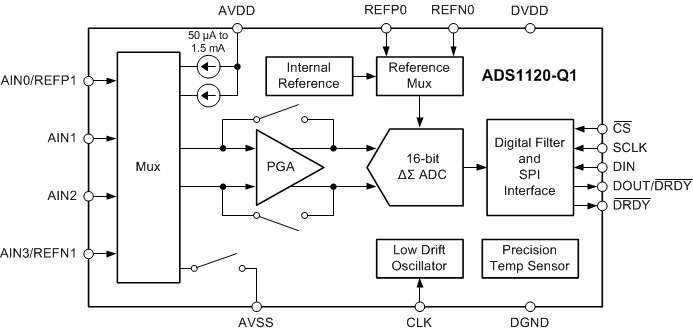
    2. 8.2 Functional Block Diagram
    3. 8.3 Feature Description
      1. 8.3.1  Multiplexer
      2. 8.3.2  Low-Noise PGA
        1. 8.3.2.1 PGA Common-Mode Voltage Requirements
        2. 8.3.2.2 Bypassing the PGA
      3. 8.3.3  Modulator
      4. 8.3.4  Digital Filter
      5. 8.3.5  Output Data Rate
      6. 8.3.6  Voltage Reference
      7. 8.3.7  Clock Source
      8. 8.3.8  Excitation Current Sources
      9. 8.3.9  Low-Side Power Switch
      10. 8.3.10 Sensor Detection
      11. 8.3.11 System Monitor
      12. 8.3.12 Offset Calibration
      13. 8.3.13 Power Supplies
      14. 8.3.14 Temperature Sensor
        1. 8.3.14.1 Converting from Temperature to Digital Codes
          1. 8.3.14.1.1 For Positive Temperatures (for Example, 50°C):
          2. 8.3.14.1.2 For Negative Temperatures (for Example, -25°C):
        2. 8.3.14.2 Converting from Digital Codes to Temperature
    4. 8.4 Device Functional Modes
      1. 8.4.1 Power-Up and Reset
      2. 8.4.2 Conversion Modes
        1. 8.4.2.1 Single-Shot Mode
        2. 8.4.2.2 Continuous Conversion Mode
      3. 8.4.3 Operating Modes
        1. 8.4.3.1 Normal Mode
        2. 8.4.3.2 Duty-Cycle Mode
        3. 8.4.3.3 Turbo Mode
        4. 8.4.3.4 Power-Down Mode
    5. 8.5 Programming
      1. 8.5.1 Serial Interface
        1. 8.5.1.1 Chip Select (CS)
        2. 8.5.1.2 Serial Clock (SCLK)
        3. 8.5.1.3 Data Ready (DRDY)
        4. 8.5.1.4 Data Input (DIN)
        5. 8.5.1.5 Data Output and Data Ready (DOUT/DRDY)
        6. 8.5.1.6 SPI Timeout
      2. 8.5.2 Data Format
      3. 8.5.3 Commands
        1. 8.5.3.1 RESET (0000 011x)
        2. 8.5.3.2 START/SYNC (0000 100x)
        3. 8.5.3.3 POWERDOWN (0000 001x)
        4. 8.5.3.4 RDATA (0001 xxxx)
        5. 8.5.3.5 RREG (0010 rrnn)
        6. 8.5.3.6 WREG (0100 rrnn)
      4. 8.5.4 Reading Data
      5. 8.5.5 Sending Commands
      6. 8.5.6 Interfacing with Multiple Devices
    6. 8.6 Register Map
      1. 8.6.1 Configuration Registers
        1. 8.6.1.1 Configuration Register 0 (offset = 00h) [reset = 00h]
        2. 8.6.1.2 Configuration Register 1 (offset = 01h) [reset = 00h]
        3. 8.6.1.3 Configuration Register 2 (offset = 02h) [reset = 00h]
        4. 8.6.1.4 Configuration Register 3 (offset = 03h) [reset = 00h]
  9. Application and Implementation
    1. 9.1 Application Information
      1. 9.1.1 Serial Interface Connections
      2. 9.1.2 Analog Input Filtering
      3. 9.1.3 External Reference and Ratiometric Measurements
      4. 9.1.4 Establishing a Proper Common-Mode Input Voltage
      5. 9.1.5 Pseudo Code Example
    2. 9.2 Typical Application
      1. 9.2.1 K-Type Thermocouple Measurement (-200°C to +1250°C)
        1. 9.2.1.1 Design Requirements
        2. 9.2.1.2 Detailed Design Procedure
        3. 9.2.1.3 Application Curves
      2. 9.2.2 3-Wire RTD Measurement (-200°C to +850°C)
        1. 9.2.2.1 Design Requirements
        2. 9.2.2.2 Detailed Design Procedure
          1. 9.2.2.2.1 Design Variations for 2-Wire and 4-Wire RTD Measurements
        3. 9.2.2.3 Application Curves
      3. 9.2.3 Bridge Measurement
        1. 9.2.3.1 Design Requirements
        2. 9.2.3.2 Detailed Design Procedure
  10. 10Power-Supply Recommendations
    1. 10.1 Power-Supply Sequencing
    2. 10.2 Power-Supply Decoupling
  11. 11Layout
    1. 11.1 Layout Guidelines
    2. 11.2 Layout Example
  12. 12器件和文档支持
    1. 12.1 文档支持
      1. 12.1.1 相关文档 
    2. 12.2 商标
    3. 12.3 静电放电警告
    4. 12.4 术语表
  13. 13机械封装和可订购信息

封装选项

机械数据 (封装 | 引脚)
散热焊盘机械数据 (封装 | 引脚)
订购信息

1 特性

  • 符合汽车应用要求
  • 具有符合 AEC-Q100 的下列结果:
    • 温度等级 1:-40°C 至 +125°C
    • 人体模型 (HBM) 静电放电 (ESD) 分类等级 2
    • 充电器件模型 (CDM) ESD 分类等级 C4B
  • 低流耗:
    占空比模式下低至 120μA(典型值)
  • 宽电源电压:2.3V 至 5.5V
  • 可编程增益:1V/V 至 128V/V
  • 可编程数据速率:5SPS 至 2kSPS
  • 16 位无噪声分辨率(20SPS 时)
  • 采用单周期稳定数字滤波器,在 20SPS 时
    实现 50Hz 和 60Hz 同步抑制
  • 两个差分输入或四个单端输入
  • 双匹配可编程电流源:50μA 至 1.5mA
  • 内部 2.048V 基准电压:漂移 5ppm/°C(典型值)
  • 内部 2% 精准振荡器
  • 内部温度传感器:精度 0.5°C(典型值)
  • SPI™- 兼容接口(模式 1)

2 应用

  • 温度传感器:
    • 热电偶
    • 电阻式温度检测器 (RTD):
      2 线、3 线或 4 线制类型
  • 桥式传感器:
    • 压力传感器
    • 应力计
  • 电池电压测量

3 说明

ADS1120-Q1 是一款精密的 16 位模数转换器 (ADC),所集成的多种特性能够降低系统成本并减少小型传感器信号测量应用中的组件数量。 这个器件具有通过灵活的输入复用器 (MUX) 实现的两个差分输入或四个单端输入,一个低噪声可编程增益放大器 (PGA),两个可编程励磁电流源,一个电压基准,一个振荡器,一个低侧开关和一个精密温度传感器。

此器件能够以高达 2000 次/秒 (SPS) 采样数据速率执行转换,并且能够在单周期内稳定。 针对噪声环境中的工业应用,当采样频率为 20SPS 时,数字滤波器能够实现 50Hz 和 60Hz 同步抑制。 其内部 PGA 提供高达 128V/V 的增益。此 PGA 使得 ADS1120-Q1 非常适用于小传感器信号测量应用,例如电阻式温度检测器 (RTD)、热电偶、热敏电阻和桥式传感器。 该器件在使用 PGA 时支持测量伪差分或全差分信号。 此外,该器件还可配置为绕过内部 PGA,同时仍提供高输入阻抗和高达 4V/V 的增益,从而实现单端测量。

在禁用 PGA 后的占空比模式下运行功耗可低至 120µA。 通过模式 1 SPI 兼容接口建立与器件之间的通信。 ADS1120-Q1 采用薄型小外形尺寸 (TSSOP)-16 封装,额定工作温度范围为 -40°C 至 +125°C。

器件信息(1)

部件号 封装 封装尺寸(标称值)
ADS1120-Q1 TSSOP (16) 5.00mm x 4.40mm
  1. 如需了解所有可用封装,请见数据表末尾的可订购产品附录。
fbd_bas683.gif