ZHCSEB1A October 2015 – November 2015 ADS1118-Q1
PRODUCTION DATA.
- 1 特性
- 2 应用
- 3 说明
- 4 修订历史记录
- 5 Device Comparison Table
- 6 Pin Configuration and Functions
- 7 Specifications
- 8 Parameter Measurement Information
- 9 Detailed Description
- 10Application and Implementation
- 11Power-Supply Recommendations
- 12Layout
- 13器件和文档支持
- 14机械、封装和可订购信息
10 Application and Implementation
NOTE
Information in the following applications sections is not part of the TI component specification, and TI does not warrant its accuracy or completeness. TI’s customers are responsible for determining suitability of components for their purposes. Customers should validate and test their design implementation to confirm system functionality.
10.1 Application Information
The ADS1118-Q1 is a precision, 16-bit ΔΣ ADC that offers many integrated features to ease the measurement of the most common sensor types including various type of temperature and bridge sensors. The following sections give example circuits and suggestions for using the ADS1118-Q1 in various situations.
10.1.1 Serial Interface Connections
The principle serial interface connections for the ADS1118-Q1 are shown in Figure 39.
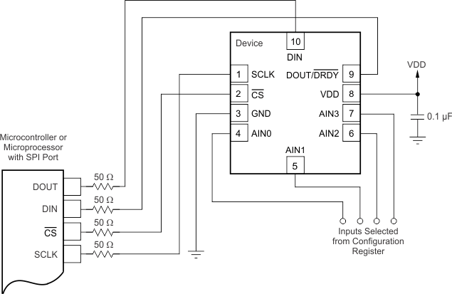 Figure 39. Typical Connections
Most microcontroller SPI peripherals operate with the ADS1118-Q1. The interface operates in SPI mode 1 where CPOL = 0 and CPHA = 1, SCLK idles low, and data are launched or changed only on SCLK rising edges; data are latched or read by the master and slave on SCLK falling edges. Details of the SPI communication protocol employed by the ADS1118-Q1 can be found in the Timing Requirements: Serial Interface section.
It is a good practice to place 50-Ω resistors in the series path to each of the digital pins to provide some short-circuit protection. Take care to still meet all SPI timing requirements because these additional series resistors along with the bus parasitic capacitances present on the digital signal lines slews the signals.
The fully-differential input of the ADS1118-Q1 is ideal for connecting to differential sources (such as thermocouples and thermistors) with a moderately low source impedance. Although the ADS1118-Q1 can read fully-differential signals, the device cannot accept negative voltages on either of its inputs because of ESD protection diodes on each pin. When an input exceeds supply or drops below ground, these diodes turn on to prevent any ESD damage to the device.
10.1.2 GPIO Ports for Communication
Most microcontrollers have programmable input/output (I/O) pins that can be set in software to act as inputs or outputs. If an SPI controller is not available, the ADS1118-Q1 can be connected to GPIO pins and the SPI bus protocol can be simulated. Using GPIO pins to generate the SPI interface requires only that the pins be configured as push or pull inputs or outputs. Furthermore, if the SCLK line is held low for more than 28 ms, communication times out. This condition means that the GPIO ports must be capable of providing SCLK pulses with no more than 28 ms between pulses.
10.1.3 Analog Input Filtering
Analog input filtering serves two purposes: first, to limit the effect of aliasing during the sampling process and second, to reduce external noise from being a part of the measurement.
As with any sampled system, aliasing can occur if proper antialias filtering is not in place. Aliasing occurs when frequency components are present in the input signal that are higher than half the sampling frequency of the ADC (also known as the Nyquist frequency). These frequency components fold back and show up in the actual frequency band of interest below half the sampling frequency. The filter response of the digital filter repeats at multiples of the sampling frequency, also known as modulator frequency f(MOD), as shown in Figure 40. Signals or noise up to a frequency where the filter response repeats are attenuated to a certain amount by the digital filter depending on the filter architecture. Any frequency components present in the input signal around the modulator frequency or multiples thereof are not attenuated and alias back into the band of interest, unless attenuated by an external analog filter.
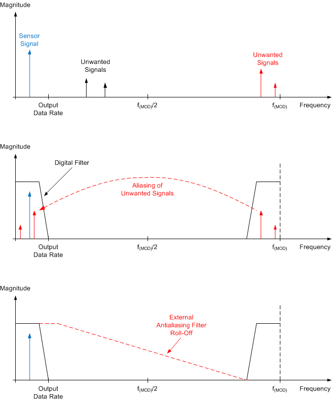 Figure 40. Effect of Aliasing
Many sensor signals are inherently band-limited; for example, the output of a thermocouple has a limited rate of change. In this case the sensor signal does not alias back into the pass-band when using a ΔΣ ADC. However, any noise pickup along the sensor wiring or the application circuitry can potentially alias into the pass band. Power line-cycle frequency and harmonics are one common noise source. External noise can also be generated from electromagnetic interference (EMI) or radio frequency interference (RFI) sources, such as nearby motors and cellular phones. Another noise source typically exists on the printed-circuit-board (PCB) itself in the form of clocks and other digital signals. Analog input filtering helps remove unwanted signals from affecting the measurement result.
A first-order, resistor-capacitor (RC) filter is, in most cases, sufficient to either totally eliminate aliasing, or to reduce the effect of aliasing to a level within the noise floor of the sensor. Ideally, any signal beyond f(MOD) / 2 is attenuated to a level below the noise floor of the ADC. The digital filter of the ADS1118-Q1 attenuates signals to a certain degree, as shown in Figure 28. In addition, noise components are usually smaller in magnitude than the actual sensor signal. Therefore, using a first-order RC filter with a cutoff frequency set at the output data rate or ten times higher is generally a good starting point for a system design.
10.1.4 Single-Ended Inputs
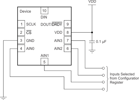
Although the ADS1118-Q1 has two differential inputs, the device can measure four single-ended signals. Figure 41 shows a single-ended connection scheme. The ADS1118-Q1 is configured for single-ended measurement by configuring the mux to measure each channel with respect to ground. Data are then read out of one input based on the selection in the Config register. The single-ended signal can range from 0 V up to positive supply or +FS, whichever is lower. Negative voltages cannot be applied to this circuit because the ADS1118-Q1 can only accept positive voltages with respect to ground. The ADS1118-Q1 does not loose linearity within the input range.
The ADS1118-Q1 offers a differential input voltage range of ±FS. The single-ended circuit shown in Figure 41, however, only uses the positive half of the ADS1118-Q1 FS input voltage range because differentially negative inputs are not produced. Because only half of the FS range is used, one bit of resolution is lost. For optimal noise performance, use differential configurations whenever possible. Differential configurations maximize the dynamic range of the ADC and provide strong attenuation of common-mode noise.
NOINDENT:
NOTE: Digital pin connections omitted for clarity.The ADS1118-Q1 also allows AIN3 to serve as a common point for measurements by adjusting the mux configuration. AIN0, AIN1, and AIN2 can all be measured with respect to AIN3. In this configuration, the ADS1118-Q1 operates with inputs where AIN3 serves as the common point. This ability improves the usable range over the single-ended configuration because negative differential voltages are allowed when GND < V(AIN3) < VDD; however, common-mode noise attenuation is not offered.
10.1.5 Connecting Multiple Devices
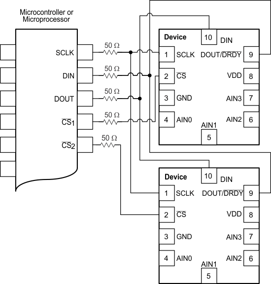
When connecting multiple ADS1118-Q1 devices to a single SPI bus, SCLK, DIN, and DOUT/DRDY can be safely shared by using a dedicated chip-select (CS) for each SPI-enabled device. By default, when CS goes high for the ADS1118-Q1, DOUT/DRDY is pulled up to VDD by a weak pullup resistor. This feature prevents DOUT/DRDY from floating near midrail and causing excess current leakage on a microcontroller input. If the PULL_UP_EN bit in the Config register is set to 0, the DOUT/DRDY pin enters a 3-state mode when CS transitions high. The ADS1118-Q1 cannot issue a data-ready pulse on DOUT/DRDY when CS is high. To evaluate when a new conversion is ready from the ADS1118-Q1 when using multiple devices, the master can periodically drop CS to the ADS1118-Q1. When CS goes low, the DOUT/DRDY pin immediately drives either high or low. If the DOUT/DRDY line drives low on a low CS, new data are currently available for clocking out at any time. If the DOUT/DRDY line drives high, no new data are available and the ADS1118-Q1 returns the last read conversion result. Valid data can be retrieved from the ADS1118-Q1 at anytime without concern of data corruption. If a new conversion becomes available during data transmission, that conversion is not available for readback until a new SPI transmission is initiated.
NOINDENT:
NOTE: Power and input connections omitted for clarity.10.1.6 Pseudo Code Example
The flow chart in Figure 43 shows a pseudo-code sequence with the required steps to set up communication between the device and a microcontroller to take subsequent readings from the ADS1118-Q1. As an example, the default Config register settings are changed to set up the device for FSR = ±0.512 V, continuous-conversion mode, and a 64-SPS data rate.
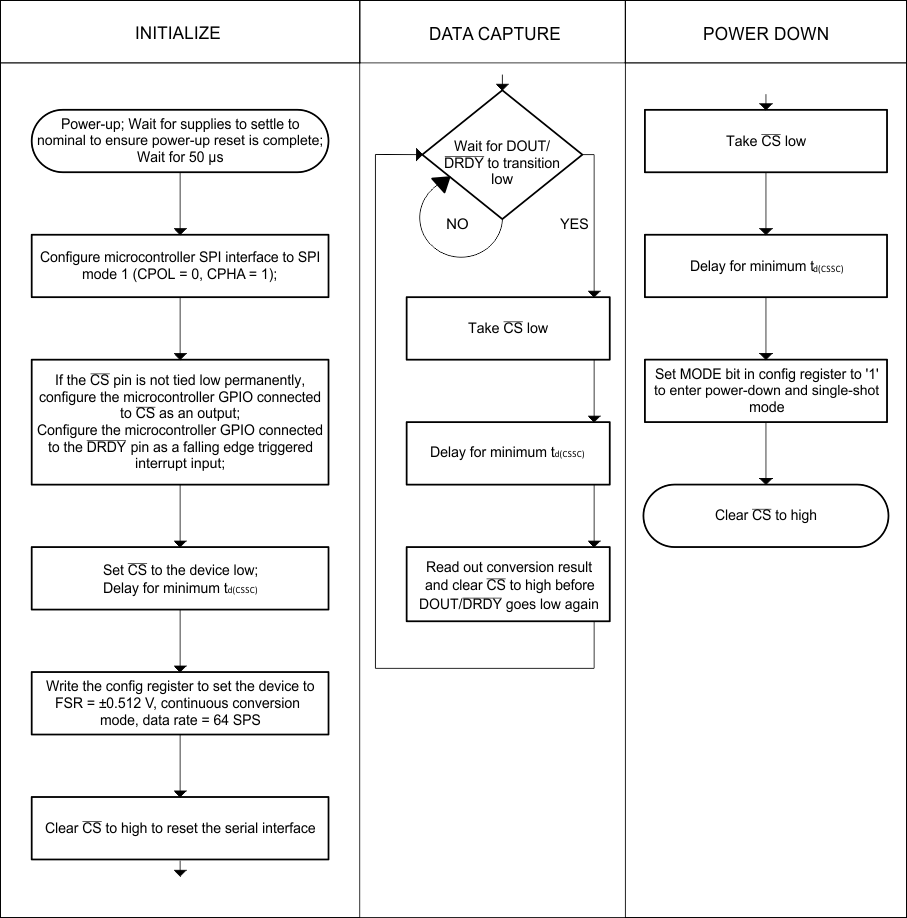 Figure 43. Pseudo-Code Example Flowchart
10.2 Typical Application
Figure 44 shows the basic connections for an independent, two-channel thermocouple measurement system when using the internal high-precision temperature sensor for cold-junction compensation. Apart from the thermocouples, the only external circuitry required are biasing resistors; first-order, low-pass, antialiasing filters; and a power-supply decoupling capacitor.
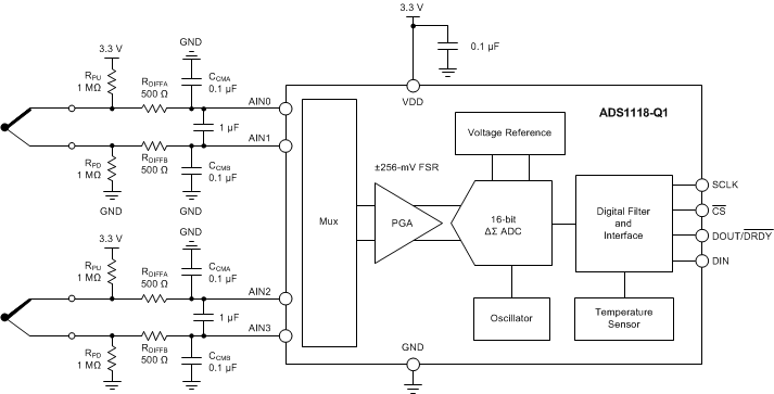 Figure 44. Two-Channel Thermocouple Measurement System
10.2.1 Design Requirements
Table 8 shows the design parameters for this application.
Table 8. Design Parameters
| DESIGN PARAMETER | VALUE |
|---|---|
| Supply voltage | 3.3 V |
| Full-scale range | ±0.256 V |
| Update rate | ≥ 100 readings per second |
| Thermocouple type | K |
| Temperature measurement range | –200°C to +1250°C |
| Measurement accuracy at TA = 25°C(1) | ±1.2°C |
10.2.2 Detailed Design Procedure
The biasing resistors (RPU and RPD) serve two purposes. The first purpose is to set the common-mode voltage of the thermocouple to within the specified voltage range of the device. The second purpose is to offer a weak pullup and pulldown to detect an open thermocouple lead. When one of the thermocouple leads fails open, the positive input is pulled to VDD and the negative input is pulled to GND. The ADC consequently reads a full-scale value that is outside the normal measurement range of the thermocouple voltage to indicate this failure condition. When choosing the values of the biasing resistors, take care so that the biasing current does not degrade measurement accuracy. The biasing current flows through the thermocouple and can cause self-heating and additional voltage drops across the thermocouple leads. Typical values for the biasing resistors range from 1 MΩ to 50 MΩ.
Although the device digital filter attenuates high-frequency components of noise, provide a first-order, passive RC filter at the inputs to further improve performance. The differential RC filter formed by RDIFFA, RDIFFB, and the differential capacitor CDIFF offers a cutoff frequency that is calculated using Equation 5. While the digital filter of the ADS1118-Q1 strongly attenuates high-frequency components of noise, provide a first-order, passive RC filter to further suppress high-frequency noise and avoid aliasing. Care must be taken when choosing the filter resistor values because the input currents flowing into and out of the device cause a voltage drop across the resistors. This voltage drop shows up as an additional offset error at the ADC inputs. Limit the filter resistor values to below 1 kΩ for best performance.
Two common-mode filter capacitors (CCMA and CCMB) are also added to offer attenuation of high-frequency, common-mode noise components. Differential capacitor CDIFF must be at least an order of magnitude (10x) larger than these common-mode capacitors because mismatches in the common-mode capacitors can convert common-mode noise into differential noise.
The highest measurement resolution is achieved when the largest potential input signal is slightly lower than the FSR of the ADC. From the design requirement, the maximum thermocouple voltage (VTC) occurs at a thermocouple temperature (TTC) of 1250°C. At this temperature, VTC = 50.644 mV, as defined in the tables published by the National Institute of Standards and Technology (NIST) using a cold-junction temperature (TCJ) of 0°C. A thermocouple produces an output voltage that is proportional to the temperature difference between the thermocouple tip and the cold junction. If the cold junction is at a temperature below 0°C, the thermocouple produces a voltage larger than 50.644 mV. The isothermal block area is constrained by the operating temperature range of the device. Therefore, the isothermal block temperature is limited to –40°C. A K-type thermocouple at TTC = 1250°C produces an output voltage of VTC = 50.644 mV – (–1.527 mV) = 52.171 mV when referenced to a cold-junction temperature of TCJ = –40°C. The device offers a full-scale range of ±0.256 V and that is what is used in this application example.
The device integrates a high-precision temperature sensor that can be used to measure the temperature of the cold junction. The temperature sensor mode is enabled by setting bit TS_MODE = 1 in the Config register. The accuracy of the overall temperature sensor depends on how accurately the ADS1118-Q1 can measure the cold junction, and hence, careful component placement and PCB layout considerations must be employed for designing an accurate thermocouple system. The ADS1118 Evaluation Module provides a good starting point and offers an example to achieve good cold-junction compensation performance. The ADS1118 Evaluation Module uses the same schematic as shown in Figure 44, except with only one thermocouple channel connected. Refer to the application note, Precision Thermocouple Measurement With the ADS1118, SBAA189, for details on how to optimize your component placement and layout to achieve good cold-junction compensation performance.
The calculation procedure to achieve cold-junction compensation can be done in several ways. A typical way is to interleave readings between the thermocouple inputs and the temperature sensor. That is, acquire one on-chip temperature result, TCJ, for every thermocouple ADC voltage measured, VTC. To account for the cold junction, first convert the temperature sensor reading within the ADS1118-Q1 to a voltage (VCJ) that is proportional to the thermocouple currently being used. This process is generally accomplished by performing a reverse lookup on the table used for the thermocouple voltage-to-temperature conversion. Adding these two voltages yields the thermocouple-compensated voltage (VActual), where VActual = VCJ + VTC. VActual is then converted to a temperature (TActual) using the same NIST lookup table. A block diagram showing this process is given in Figure 45. Refer to the application note, Precision Thermocouple Measurement With the ADS1118, SBAA189, for a detailed explanation of this method.
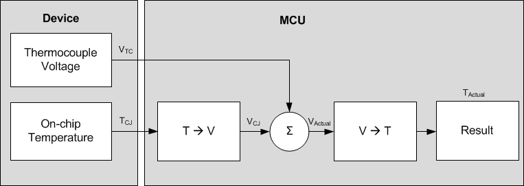 Figure 45. Software-Flow Block Diagram
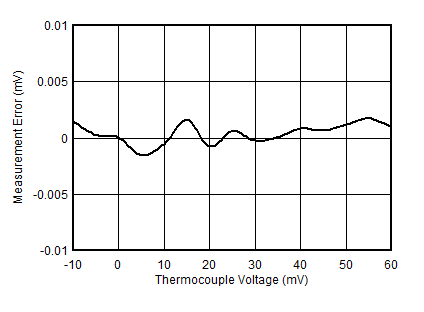
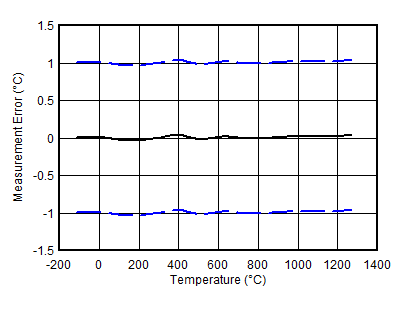
Figure 46 and Figure 47 show the measurement results. The measurements are taken at TA = TCJ = 25°C. A system offset calibration is performed at TTC = 25°C that equates to VTC = 0 V when TCJ = 25°C. No gain calibration was performed during the measurements. The data in Figure 46 are taken using a precision voltage source as the input signal instead of a thermocouple. The solid black line in Figure 47 is the respective temperature measurement error and is calculated from the data in Figure 46 using the NIST tables. The solid black line in Figure 47 is the measurement error due to the ADC gain and nonlinearity error. The dashed blue lines in Figure 47 include the guard band for the temperature sensor inaccuracy (±1°C), in addition to the device gain and nonlinearity error. Note that the measurement results in Figure 46 and Figure 47 do not account for the thermocouple inaccuracy that must also be considered while designing a thermocouple measurement system.
10.2.3 Application Curves
