SNAS468D September 2008 – December 2014 ADC161S626
PRODUCTION DATA.
- 1 Features
- 2 Applications
- 3 Description
- 4 Revision History
- 5 Pin Configuration and Functions
- 6 Specifications
- 7 Detailed Description
- 8 Application and Implementation
- 9 Power Supply Recommendations
- 10Layout
- 11Device and Documentation Support
- 12Mechanical, Packaging, and Orderable Information
8 Application and Implementation
NOTE
Information in the following applications sections is not part of the TI component specification, and TI does not warrant its accuracy or completeness. TI’s customers are responsible for determining suitability of components for their purposes. Customers should validate and test their design implementation to confirm system functionality.
8.1 Application Information
The following sections outline the design principles of data acquisition system based on the ADC161S626.
8.2 Typical Application
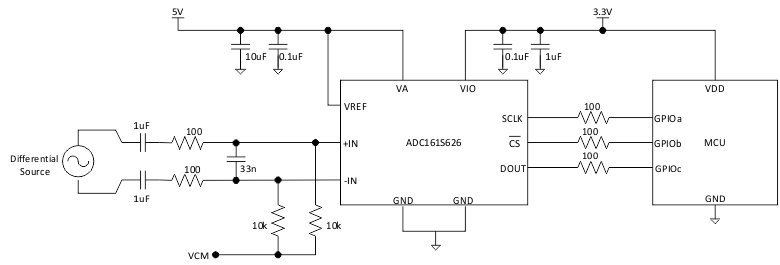 Figure 48. Low Cost, Low Power Data Acquisition System
Figure 48 shows a typical connection diagram for the ADC161S626 operating at VA of 5 V. VREF is connected to a 2.5-V shunt reference, the LM4020-2.5, to define the analog input range of the ADC161S626 independent of supply variation on the 5-V supply line. The VREF pin should be de-coupled to the ground plane by a 0.1-µF ceramic capacitor and a tantalum capacitor of 10 µF. It is important that the 0.1-µF capacitor be placed as close as possible to the VREF pin while the placement of the tantalum capacitor is less critical. It is also recommended that the VA and VIO pins of the ADC161S626 be de-coupled to ground by a 0.1-µF ceramic capacitor in parallel with a 10-µF tantalum capacitor.
8.2.1 Design Requirements
A positive supply only data acquisition system capable of digitizing differential signals ranging from –5 V to 5 V (V+IN – V-IN), BW = 10 kHz, and a throughput of 250 kSPS (FS).
The ADC161S626 has to interface to an MCU whose supply is set at 3.3 V.
8.2.2 Detailed Design Procedure
The signal range requirement forces the design to use 5 V as VREF potential. This, in turn, forces the VA to be no less than 5 V as well.
The requirement of interfacing to the MCU which is powered by 3.3-V supply, forces the choice of 3.3 V as a VD supply.
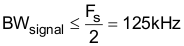
Sampling is in fact a modulation process which may result in aliasing of the input signal, if the input signal is not adequately band limited. In order to avoid the aliasing the Nyquist criterion has to be met:
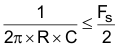
Therefore it is necessary to place an anti-aliasing filter at the input of the ADC. The filter may be single pole low pass filter whose pole location has to satisfy:
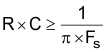
With Fs = 250 kHz, a good choice for the single pole filter is:
R = 100
C = 33 nF
This reduces the input BWsignal = 48 kHz.
The capacitor at the inputs of the device provides not only the filtering of the input signal, but it also absorbs the charge kick-back from the ADC. The kick-back is the result of the internal switches opening at the end of the acquisition period.
The common mode level of the ADC inputs has to be set by the external bias source. The VCM bias has to be isolated from the inputs by a large resistance in order to avoid input signal attenuation.
The VA and VIO sources are already separated in this example, due to the design requirements. This also benefits the overall performance of the ADC, as the potentially noisy VIO supply does not contaminate the VA. In the same vain, further consideration could be given to the SPI interface, especially when the master MCU is capable of producing fast rising edges on the digital bus signals. Inserting small resistances in the digital signal path may help in reducing the ground bounce, and thus improve the overall noise performance of the system.
8.2.3 Application Curve
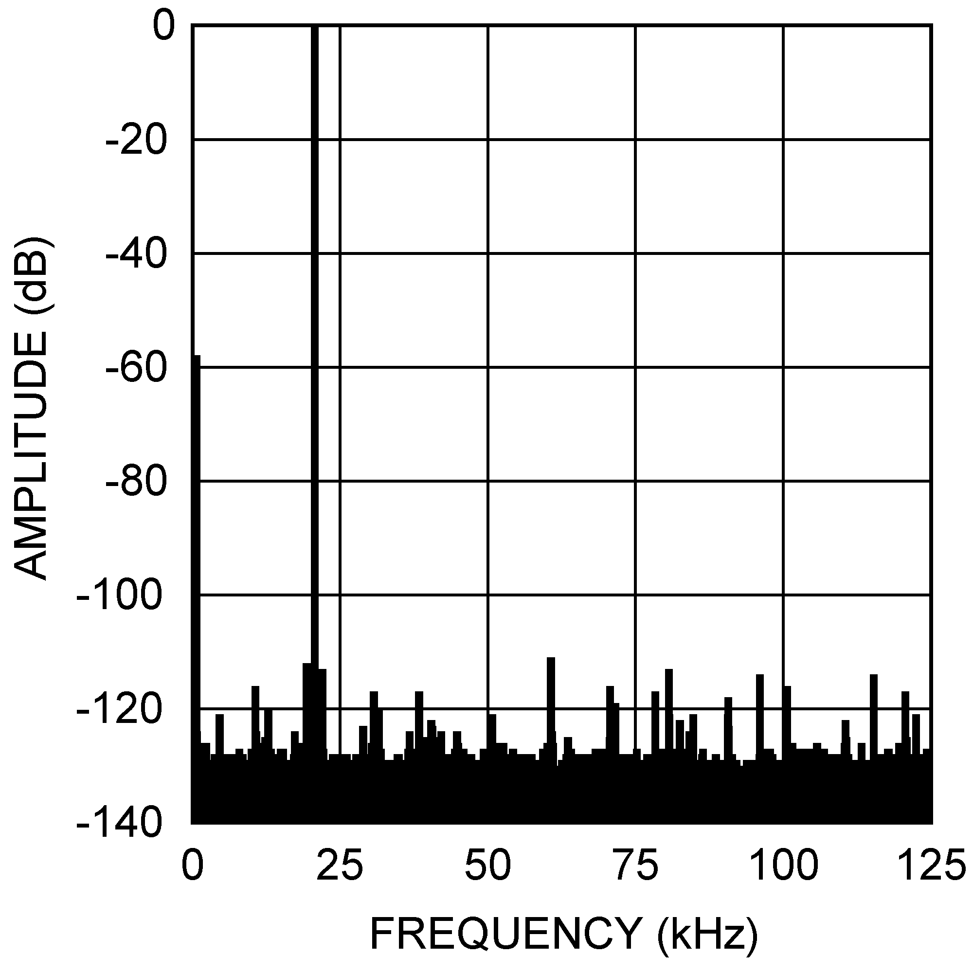 Figure 49. Spectral Response