SNAS500Q May 2010 – May 2017 ADC12D1800
PRODUCTION DATA.
- 1 Device Overview
- 2 Revision History
- 3 Pin Configuration and Functions
-
4 Specifications
- 4.1 Absolute Maximum Ratings
- 4.2 ESD Ratings
- 4.3 Recommended Operating Conditions
- 4.4 Thermal Information
- 4.5 Converter Electrical Characteristics: Static Converter Characteristics
- 4.6 Converter Electrical Characteristics: Dynamic Converter Characteristics
- 4.7 Converter Electrical Characteristics: Analog Input and Output and Reference Characteristics
- 4.8 Converter Electrical Characteristics: I-Channel to Q-Channel Characteristics
- 4.9 Converter Electrical Characteristics: Sampling Clock Characteristics
- 4.10 Converter Electrical Characteristics: AutoSync Feature Characteristics
- 4.11 Converter Electrical Characteristics: Digital Control and Output Pin Characteristics
- 4.12 Converter Electrical Characteristics: Power Supply Characteristics
- 4.13 Converter Electrical Characteristics: AC Electrical Characteristics
- 4.14 Converter Timing Requirements: Serial Port Interface
- 4.15 Converter Switching Characteristics: Calibration
- 4.16 Typical Characteristics
-
5 Detailed Description
- 5.1 Overview
- 5.2 Functional Block Diagram
- 5.3 Feature Description
- 5.4 Device Functional Modes
- 5.5
Programming
- 5.5.1
Control Modes
- 5.5.1.1
Non-Extended Control Mode
- 5.5.1.1.1 Dual Edge Sampling Pin (DES)
- 5.5.1.1.2 Non-Demultiplexed Mode Pin (NDM)
- 5.5.1.1.3 Dual Data Rate Phase Pin (DDRPh)
- 5.5.1.1.4 Calibration Pin (CAL)
- 5.5.1.1.5 Calibration Delay Pin (CalDly)
- 5.5.1.1.6 Power Down I-channel Pin (PDI)
- 5.5.1.1.7 Power Down Q-channel Pin (PDQ)
- 5.5.1.1.8 Test Pattern Mode Pin (TPM)
- 5.5.1.1.9 Full-Scale Input Range Pin (FSR)
- 5.5.1.1.10 AC/DC-Coupled Mode Pin (VCMO)
- 5.5.1.1.11 LVDS Output Common-mode Pin (VBG)
- 5.5.1.2 Extended Control Mode
- 5.5.1.1
Non-Extended Control Mode
- 5.5.1
Control Modes
- 5.6 Register Maps
- 6 Application and Implementation
- 7 Power Supply Recommendations
- 8 Layout
- 9 Device and Documentation Support
- 10Mechanical, Packaging, and Orderable Information
4 Specifications
4.1 Absolute Maximum Ratings
(see (1)(2))| MIN | MAX | UNIT | ||
|---|---|---|---|---|
| Supply voltage (VA, VTC, VDR, VE) | 2.2 | V | ||
| Supply difference max(VA/TC/DR/E) − min(VA/TC/DR/E) |
0 | 100 | mV | |
| Voltage on any input pin (except VIN±) |
−0.15 | (VA + 0.15) | V | |
| VIN± voltage range | –0.5 | 2.5 | V | |
| Ground difference max(GNDTC/DR/E) -min(GNDTC/DR/E) |
0 | 100 | mV | |
| Input current at any pin(3) | –50 | 50 | mA | |
| ADC12D1800 package power dissipation at TA ≤ 65°C(3) | 4.95 | W | ||
| Storage temperature, Tstg | –65 | 150 | °C | |
(1) Absolute Maximum Ratings indicate limits beyond which damage to the device may occur. There is no specification of operation at the Absolute Maximum Ratings. Section 4.3 indicates conditions for which the device is functional, but do not ensure specific performance limits. For ensured specifications and test conditions, see the Electrical Characteristics. The ensured specifications apply only for the test conditions listed. Some performance characteristics may degrade when the device is not operated under the listed test conditions.
(2) All voltages are measured with respect to GND = GNDTC = GNDDR = GNDE = 0V, unless otherwise specified.
(3) When the input voltage at any pin exceeds the power supply limits (for example, less than GND or greater than VA), the current at that pin should be limited to 50 mA. In addition, over-voltage at a pin must adhere to the maximum voltage limits. Simultaneous over-voltage at multiple pins requires adherence to the maximum package power dissipation limits. These dissipation limits are calculated using JEDEC JESD51-7 thermal model. Higher dissipation may be possible based on specific customer thermal situation and specified package thermal resistances from junction to case.
4.2 ESD Ratings
| VALUE | UNIT | |||
|---|---|---|---|---|
| V(ESD) | Electrostatic discharge | Human body model (HBM), per ANSI/ESDA/JEDEC JS-001(1) | ±2500 | V |
| Charged device model (CDM), per JEDEC specification JESD22-C101(2) | ±1000 | |||
| Machine model (MM) | ±250 | |||
(1) JEDEC document JEP155 states that 500-V HBM allows safe manufacturing with a standard ESD control process.
(2) JEDEC document JEP157 states that 250-V CDM allows safe manufacturing with a standard ESD control process.
4.3 Recommended Operating Conditions
(see (1)(2))| MIN | MAX | UNIT | ||
|---|---|---|---|---|
| Ambient temperature range | TA ADC12D1800 (Standard JEDEC thermal model) |
−40 | 50 | °C |
| TA ADC12D1800 (Enhanced thermal model/heatsink) |
−40 | 85 | °C | |
| TJ Junction temperature range (applies only to maximum operating speed) | 120 | °C | ||
| Supply voltage (VA, VTC, VE) | +1.8 | +2.0 | V | |
| Driver supply voltage (VDR) | +1.8 | VA | V | |
| VIN+/- Voltage range(3) | –0.4 | 2.4 (DC-coupled) |
V | |
| VIN+/- Differential voltage range(4) | 1.0 (DC-coupled at 100% duty cycle) 2.0 (DC-coupled at 20% duty cycle) 2.8 (DC-coupled at 10% duty cycle) |
V | ||
| VIN+/- Current range(3) | –50 | ±50 peak (A.C.-coupled) |
mA | |
| VIN+/- Power | (maintaining common mode voltage, A.C.-coupled) |
15.3 | dBm | |
| (not maintaining common mode voltage, A.C.-coupled) |
17.1 | |||
| Ground difference max(GNDTC/DR/E) – min(GNDTC/DR/E) |
0 | V | ||
| CLK+/- Voltage range | 0 | VA | V | |
| Differential CLK amplitude VP–P | 0.4 | 2 | V | |
| Common mode input voltage VCMI | VCMO - 150 | VCMO + 150 | mV | |
(1) Absolute Maximum Ratings indicate limits beyond which damage to the device may occur. There is no specification of operation at the Absolute Maximum Ratings. Section 4.3 indicates conditions for which the device is functional, but do not ensure specific performance limits. For ensured specifications and test conditions, see the Electrical Characteristics. The ensured specifications apply only for the test conditions listed. Some performance characteristics may degrade when the device is not operated under the listed test conditions.
(2) All voltages are measured with respect to GND = GNDTC = GNDDR = GNDE = 0V, unless otherwise specified.
(3) Proper common mode voltage must be maintained to ensure proper output codes, especially during input overdrive.
(4) This rating is intended for DC-coupled applications; the voltages listed may be safely applied to VIN+/- for the life-time duty-cycle of the part.
4.4 Thermal Information
| THERMAL METRIC(1) | ADC12D1800 | UNIT | |
|---|---|---|---|
| NXA (BGA) | |||
| 292 PINS | |||
| RθJA | Junction-to-ambient thermal resistance | 16 | °C/W |
| RθJC(top) | Junction-to-case (top) thermal resistance | 2.9 | °C/W |
| RθJC(bot) | Junction-to-case (bottom) thermal resistance | 2.5 | °C/W |
(1) For more information about traditional and new thermal metrics, see the Semiconductor and IC Package Thermal Metrics application report, SPRA953.
4.5 Converter Electrical Characteristics: Static Converter Characteristics
Unless otherwise specified, the following apply after calibration for VA = VDR = VTC = VE = +1.9V; I- and Q-channels, AC-coupled, unused channel terminated to AC ground, FSR Pin = High; CL = 10 pF; Differential, AC coupled Sine Wave Sampling Clock, fCLK = 1.8 GHz at 0.5 VP-P with 50% duty cycle (as specified); VBG = Floating; Extended Control Mode with Register 6h written to 1C00h; Rext = Rtrim = 3300Ω ± 0.1%; Analog Signal Source Impedance = 100Ω Differential; 1:2 Demultiplex Non-DES Mode; Duty Cycle Stabilizer on. Max limits are TA = TMIN to TMAX, TJ < 105°C, unless otherwise noted.(1) (2)(3)| PARAMETER | TEST CONDITIONS | TYP | MAX | UNIT | |
|---|---|---|---|---|---|
| Resolution with no missing codes | TA = TMIN to TMAX, TJ < 105°C | 12 | bits | ||
| INL | Integral non-linearity (Best fit) |
1 MHz DC-coupled over-ranged sine wave | ±2.5 | LSB | |
| DNL | Differential non-linearity | 1 MHz DC-coupled over-ranged sine wave | ±0.4 | LSB | |
| VOFF | Offset error | 5 | LSB | ||
| VOFF_ADJ | Input offset adjustment range | Extended Control Mode | ±45 | mV | |
| PFSE | Positive full-scale error | See (4) | ±25 | mV | |
| NFSE | Negative full-scale error | See (4) | ±25 | mV | |
| Out-of-range output code (5) | (VIN+) − (VIN−) > + full scale | 4095 | |||
| (VIN+) − (VIN−) < − full scale | 0 | ||||
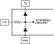
(1) The analog inputs, labeled I/O, are protected as shown below. Input voltage magnitudes beyond the Absolute Maximum Ratings may damage this device.

(2) To ensure accuracy, it is required that VA, VTC, VE and VDR be well-bypassed. Each supply pin must be decoupled with separate bypass capacitors.
(3) Typical figures are at TA = 25°C, and represent most likely parametric norms. Test limits are specified to TI's AOQL (Average Outgoing Quality Level).
(4) Calculation of Full-Scale Error for this device assumes that the actual reference voltage is exactly its nominal value. Full-Scale Error for this device, therefore, is a combination of Full-Scale Error and Reference Voltage Error. See Figure 4-1. For relationship between Gain Error and Full-Scale Error, see Specification Definitions for Gain Error.
(5) This parameter is ensured by design and is not tested in production.
4.6 Converter Electrical Characteristics: Dynamic Converter Characteristics
Limits are TA = TMIN to TMAX, TJ < 105°C| PARAMETER | TEST CONDITIONS | MIN | TYP | MAX | UNIT | ||
|---|---|---|---|---|---|---|---|
| FPBW | Full power bandwidth | Non-DES Mode | 2.8 | GHz | |||
| DESI, DESQ Mode | 1.25 | GHz | |||||
| DESIQ Mode | 1.75 | GHz | |||||
| Gain flatness | Non-DES Mode | D.C. to Fs/2 | 0.5 | dB | |||
| D.C. to Fs | 1.2 | dB | |||||
| DESI, DESQ Mode | D.C. to Fs/2 | 4.0 | dB | ||||
| DESIQ Mode | D.C. to Fs/2 | 3.6 | dB | ||||
| CER | Code error rate | 10-18 | Error/Sample | ||||
| NPR | Noise power ratio | See (1) | 48.5 | dB | |||
| IMD3 | 3rd order intermodulation distortion | DESIQ Mode FIN1 = 1212.52MHz at -7dBFS FIN2 = 1217.52 MHz at -7dBFS |
-61 | dBFS | |||
| -54 | dBc | ||||||
| Noise floor density | 50Ω single-ended termination, DES Mode | -153.5 | dBm/Hz | ||||
| -152.5 | dBFS/Hz | ||||||
| Wideband input, DES Mode(2) | -152.6 | dBm/Hz | |||||
| -151.6 | dBFS/Hz | ||||||
| NON-DES MODE(3)(4) | |||||||
| ENOB | Effective Number of Bits | AIN = 125 MHz at -0.5 dBFS | 9.4 | bits | |||
| AIN = 248 MHz at -0.5 dBFS | 8.4 | 9.2 | bits | ||||
| AIN = 498 MHz at -0.5 dBFS | 8.4 | 9.1 | bits | ||||
| AIN = 1147 MHz at -0.5 dBFS | 8.5 | bits | |||||
| AIN = 1448 MHz at -0.5 dBFS | 8.4 | bits | |||||
| SINAD | Signal-to-Noise Plus Distortion Ratio | AIN = 125 MHz at -0.5 dBFS | 58 | dB | |||
| AIN = 248 MHz at -0.5 dBFS | 52.1 | 57.3 | dB | ||||
| AIN = 498 MHz at -0.5 dBFS | 52.1 | 56.3 | dB | ||||
| AIN = 1147 MHz at -0.5 dBFS | 52.9 | dB | |||||
| AIN = 1448 MHz at -0.5 dBFS | 52.5 | dB | |||||
| SNR | Signal-to-Noise Ratio | AIN = 125 MHz at -0.5 dBFS | 58.6 | dB | |||
| AIN = 248 MHz at -0.5 dBFS | 52.9 | 57.8 | dB | ||||
| AIN = 498 MHz at -0.5 dBFS | 52.9 | 57.3 | dB | ||||
| AIN = 1147 MHz at -0.5 dBFS | 53.9 | dB | |||||
| AIN = 1448 MHz at -0.5 dBFS | 53.1 | dB | |||||
| THD | Total Harmonic Distortion | AIN = 125 MHz at -0.5 dBFS | -68.5 | dB | |||
| AIN = 248 MHz at -0.5 dBFS | -60 | -66.6 | dB | ||||
| AIN = 498 MHz at -0.5 dBFS | -60 | -63.2 | dB | ||||
| AIN = 1147 MHz at -0.5 dBFS | -59.5 | dB | |||||
| AIN = 1448 MHz at -0.5 dBFS | -61.1 | dB | |||||
| 2nd Harm | Second Harmonic Distortion | AIN = 125 MHz at -0.5 dBFS | 73 | dBc | |||
| AIN = 248 MHz at -0.5 dBFS | 87 | dBc | |||||
| AIN = 498 MHz at -0.5 dBFS | 70 | dBc | |||||
| AIN = 1147 MHz at -0.5 dBFS | 62 | dBc | |||||
| AIN = 1448 MHz at -0.5 dBFS | 66 | dBc | |||||
| 3rd Harm | Third Harmonic Distortion | AIN = 125 MHz at -0.5 dBFS | 76.8 | dBc | |||
| AIN = 248 MHz at -0.5 dBFS | 67.4 | dBc | |||||
| AIN = 498 MHz at -0.5 dBFS | 66.3 | dBc | |||||
| AIN = 1147 MHz at -0.5 dBFS | 63 | dBc | |||||
| AIN = 1448 MHz at -0.5 dBFS | 63.6 | dBc | |||||
| SFDR | Spurious-Free Dynamic Range | AIN = 125 MHz at -0.5 dBFS | 73 | dBc | |||
| AIN = 248 MHz at -0.5 dBFS | 67.5 | 58 | dBc | ||||
| AIN = 498 MHz at -0.5 dBFS | 66.1 | 58 | dBc | ||||
| AIN = 1147 MHz at -0.5 dBFS | 60.2 | dBc | |||||
| AIN = 1448 MHz at -0.5 dBFS | 60.3 | dBc | |||||
| DES MODE(3)(4) (5) | |||||||
| ENOB | Effective number of bits | AIN = 125 MHz at -0.5 dBFS | 8.9 | bits | |||
| AIN = 248 MHz at -0.5 dBFS | 8.8 | 8.4 | bits | ||||
| AIN = 498 MHz at -0.5 dBFS | 8.6 | bits | |||||
| AIN = 1147 MHz at -0.5 dBFS | 8 | bits | |||||
| AIN = 1448 MHz at -0.5 dBFS | 8 | bits | |||||
| SINAD | Signal-to-noise plus distortion ratio | AIN = 125 MHz at -0.5 dBFS | 55.6 | dB | |||
| AIN = 248 MHz at -0.5 dBFS | 54.8 | 52.1 | dB | ||||
| AIN = 498 MHz at -0.5 dBFS | 53.8 | dB | |||||
| AIN = 1147 MHz at -0.5 dBFS | 50 | dB | |||||
| AIN = 1448 MHz at -0.5 dBFS | 49.8 | dB | |||||
| SNR | Signal-to-noise ratio | AIN = 125 MHz at -0.5 dBFS | 55.8 | dB | |||
| AIN = 248 MHz at -0.5 dBFS | 55.3 | 52.9 | dB | ||||
| AIN = 498 MHz at -0.5 dBFS | 54.5 | dB | |||||
| AIN = 1147 MHz at -0.5 dBFS | 50.4 | dB | |||||
| AIN = 1448 MHz at -0.5 dBFS | 50.1 | dB | |||||
| THD | Total harmonic distortion | AIN = 125 MHz at -0.5 dBFS | -67.8 | dB | |||
| AIN = 248 MHz at -0.5 dBFS | -65 | -60 | dB | ||||
| AIN = 498 MHz at -0.5 dBFS | -62 | dB | |||||
| AIN = 1147 MHz at -0.5 dBFS | -60.6 | dB | |||||
| AIN = 1448 MHz at -0.5 dBFS | -61.9 | dB | |||||
| 2nd Harm | Second harmonic distortion | AIN = 125 MHz at -0.5 dBFS | 78 | dBc | |||
| AIN = 248 MHz at -0.5 dBFS | 74.4 | dBc | |||||
| AIN = 498 MHz at -0.5 dBFS | 72.5 | dBc | |||||
| AIN = 1147 MHz at -0.5 dBFS | 70.5 | dBc | |||||
| AIN = 1448 MHz at -0.5 dBFS | 72.8 | dBc | |||||
| 3rd Harm | Third harmonic distortion | AIN = 125 MHz at -0.5 dBFS | 72.6 | dBc | |||
| AIN = 248 MHz at -0.5 dBFS | 66.5 | dBc | |||||
| AIN = 498 MHz at -0.5 dBFS | 63.2 | dBc | |||||
| AIN = 1147 MHz at -0.5 dBFS | 61.8 | dBc | |||||
| AIN = 1448 MHz at -0.5 dBFS | 63.8 | dBc | |||||
| SFDR | Spurious-free dynamic range | AIN = 125 MHz at -0.5 dBFS | 58.9 | dBc | |||
| AIN = 248 MHz at -0.5 dBFS | 60.4 | 58 | dBc | ||||
| AIN = 498 MHz at -0.5 dBFS | 60.5 | dBc | |||||
| AIN = 1147 MHz at -0.5 dBFS | 56.7 | dBc | |||||
| AIN = 1448 MHz at -0.5 dBFS | 55.6 | dBc | |||||
(1) The NPR was measured using an Agilent N6030A Arbitrary Waveform Generator (ARB) to generate the input signal. See the Wideband Performance for an example spectrum. The "noise" portion of the signal was created by tones spaced at 500 kHz and the "notch" was a 25 MHz absence of tones centered at 320 MHz. The bandwidth of this equipment is only 500 MHz, so the final reported NPR was extrapolated from the measured NPR as if the entire Nyquist band were occupied with noise.
(2) The Noise Floor Density was measured for two conditions: the analog input terminated with 50Ω, and in the presence of a 500 MHz wideband noise signal with total power just below the maximum input level to the ADC. In both cases, the spurs at DC, Fs/4 and Fs/2 were not included in the noise floor calculation. The power over the entire Nyquist band (except for the noise signal) was integrated and the average number is reported.
(3) The Dynamic Specifications are ensured for room to hot ambient temperature only (25°C to 85°C). Refer to the plots of the dynamic performance vs. temperature in the Typical Performance Plots to see typical performance from cold to room temperature (-40°C to 25°C).
(4) The Fs/2 spur was removed from all the dynamic performance specifications.
(5) These measurements were taken in Extended Control Mode (ECM) with the DES Timing Adjust feature enabled (Addr: 7h). This feature is used to reduce the interleaving timing spur amplitude, which occurs at fs/2-fin, and thereby increase the SFDR, SINAD and ENOB.
4.7 Converter Electrical Characteristics: Analog Input and Output and Reference Characteristics
Limits are TA = TMIN to TMAX, TJ < 105°C| PARAMETER | TEST CONDITIONS | MIN | TYP | MAX | UNIT | ||
|---|---|---|---|---|---|---|---|
| ANALOG INPUTS | |||||||
| VIN_FSR | Analog differential input full scale range | Non-Extended Control Mode | FSR Pin High | 740 | 800 | 860 | mVP-P |
| Extended Control Mode | FM(14:0) = 4000h (default) | 800 | mVP-P | ||||
| FM(14:0) = 7FFFh | 1000 | mVP-P | |||||
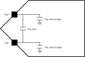
| CIN | Analog input capacitance, non-DES mode (1) (2) | Differential | 0.02 | pF | |||
| Each input pin to ground | 1.6 | pF | |||||
| Analog input capacitance, DES mode (1) (2) | Differential | 0.08 | pF | ||||
| Each input pin to ground | 2.2 | pF | |||||
| RIN | Differential input resistance | 91 | 100 | 109 | Ω | ||
| COMMON MODE OUTPUT | |||||||
| VCMO | Common mode output voltage | ICMO = ±100 µA | 1.15 | 1.25 | 1.35 | V | |
| TC_VCMO | Common mode output voltage temperature coefficient | ICMO = ±100 µA | 38 | ppm/°C | |||
| VCMO_LVL | VCMO input threshold to set DC-coupling Mode |
0.63 | V | ||||
| CL_VCMO | Maximum VCMO load capacitance | (1) | 80 | pF | |||
| BANDGAP REFERENCE | |||||||
| VBG | Bandgap reference output voltage | IBG = ±100 µA | 1.15 | 1.25 | 1.35 | V | |
| TC_VBG | Bandgap reference voltage temperature coefficient | IBG = ±100 µA | 32 | ppm/°C | |||
| CL_VBG | Maximum bandgap reference load capacitance | (1) | 80 | pF | |||
(1) This parameter is ensured by design and is not tested in production.
(2) The differential and pin-to-ground input capacitances are lumped capacitance values from design; they are defined as shown below.

4.8 Converter Electrical Characteristics: I-Channel to Q-Channel Characteristics
| PARAMETER | TEST CONDITIONS | TYP | LIM | UNIT | |
|---|---|---|---|---|---|
| Offset match | 2 | LSB | |||
| Positive full-scale match | Zero offset selected in Control Register |
2 | LSB | ||
| Negative full-scale match | Zero offset selected in Control Register |
2 | LSB | ||
| Phase matching (I, Q) | fIN = 1.0 GHz | < 1 | Degree | ||
| X-TALK | Crosstalk from I-channel (Aggressor) to Q-channel (Victim) | Aggressor = 867 MHz F.S. Victim = 100 MHz F.S. |
−70 | dB | |
| Crosstalk from Q-channel (Aggressor) to I-channel (Victim) | Aggressor = 867 MHz F.S. Victim = 100 MHz F.S. |
−70 | dB | ||
4.9 Converter Electrical Characteristics: Sampling Clock Characteristics
Limits are TA = TMIN to TMAX, TJ < 105°C| PARAMETER | TEST CONDITIONS | MIN | TYP | MAX | UNIT | |
|---|---|---|---|---|---|---|
| VIN_CLK | Differential sampling clock input level (1) | Sine wave clock Differential Peak-to-peak |
0.4 | 0.6 | 2.0 | VP-P |
| Square wave clock Differential peak-to-peak |
0.4 | 0.6 | 2.0 | VP-P | ||
| CIN_CLK | Sampling clock input capacitance (2) |
Differential | 0.1 | pF | ||
| Each input to ground | 1 | pF | ||||
| RIN_CLK | Sampling clock differential input resistance | 100 | Ω | |||
(1) This parameter is ensured by design and/or characterization and is not tested in production.
(2) This parameter is ensured by design and is not tested in production.
4.10 Converter Electrical Characteristics: AutoSync Feature Characteristics
| PARAMETER | TEST CONDITIONS | MIN | TYP | MAX | UNIT | |
|---|---|---|---|---|---|---|
| VIN_RCLK | Differential RCLK input level | Differential peak-to-peak | 360 | mVP-P | ||
| CIN_RCLK | RCLK input capacitance | Differential | 0.1 | pF | ||
| Each input to ground | 1 | pF | ||||
| RIN_RCLK | RCLK differential input resistance | 100 | Ω | |||
| IIH_RCLK | Input leakage current; VIN = VA |
22 | µA | |||
| IIL_RCLK | Input leakage current; VIN = GND |
-33 | µA | |||
| VO_RCOUT | Differential RCOut Output Voltage | 360 | mV | |||
4.11 Converter Electrical Characteristics: Digital Control and Output Pin Characteristics
Limits are TA = TMIN to TMAX, TJ < 105°C| PARAMETER | TEST CONDITIONS | MIN | TYP | MAX | UNIT | |
|---|---|---|---|---|---|---|
| DIGITAL CONTROL PINS (DES, CalDly, CAL, PDI, PDQ, TPM, NDM, FSR, DDRPh, ECE, SCLK, SDI, SCS) | ||||||
| VIH | Logic high input voltage | 0.7×VA | 0.3×VA | V | ||
| VIL | Logic low input voltage | |||||
| IIH | Input leakage current; VIN = VA |
0.02 | μA | |||
| IIL | Input leakage current; VIN = GND |
FSR, CalDly, CAL, NDM, TPM, DDRPh, DES | -0.02 | μA | ||
| SCS, SCLK, SDI | -17 | μA | ||||
| PDI, PDQ, ECE | -38 | μA | ||||
| CIN_DIG | Digital control pin input capacitance (1) | Measured from each control pin to GND | 1.5 | pF | ||
| DIGITAL OUTPUT PINS (Data, DCLKI, DCLKQ, ORI, ORQ) | ||||||
| VOD | LVDS differential output voltage | VBG = Floating, OVS = High | 400 | 630 | 800 | mVP-P |
| VBG = Floating, OVS = Low | 230 | 460 | 630 | mVP-P | ||
| VBG = VA, OVS = High | 670 | mVP-P | ||||
| VBG = VA, OVS = Low | 500 | mVP-P | ||||
| ΔVO DIFF | Change in LVDS output swing between logic levels | ±1 | mV | |||
| VOS | Output offset voltage | VBG = Floating | 0.8 | V | ||
| VBG = VA | 1.2 | V | ||||
| ΔVOS | Output offset voltage change between logic levels | ±1 | mV | |||
| IOS | Output short circuit current | VBG = Floating; D+ and D− connected to 0.8V |
±4 | mA | ||
| ZO | Differential output impedance | 100 | Ω | |||
| VOH | Logic high output level | CalRun, IOH = −100 µA, (2)
SDO, IOH = −400 µA (2) |
1.65 | V | ||
| VOL | Logic low output level | CalRun, IOL = 100 µA, (2)
SDO, IOL = 400 µA (2) |
0.15 | V | ||
| DIFFERENTIAL DCLK RESET PINS (DCLK_RST) | ||||||
| VCMI_DRST | DCLK_RST common mode input voltage | 1.25 | V | |||
| VID_DRST | Differential DCLK_RST input voltage | VIN_CLK | VP-P | |||
| RIN_DRST | Differential DCLK_RST input resistance | (1) | 100 | Ω | ||
(1) This parameter is ensured by design and is not tested in production.
(2) This parameter is ensured by design and/or characterization and is not tested in production.
4.12 Converter Electrical Characteristics: Power Supply Characteristics
Limits are TA = TMIN to TMAX, TJ < 105°C| PARAMETER | TEST CONDITIONS | TYP | MAX | UNIT | ||
|---|---|---|---|---|---|---|
| IA | Analog supply current | PDI = PDQ = Low | 1345 | mA | ||
| PDI = Low; PDQ = High | 730 | mA | ||||
| PDI = High; PDQ = Low | 730 | mA | ||||
| PDI = PDQ = High | 15 | mA | ||||
| ITC | Track-and-hold and clock supply current | PDI = PDQ = Low | 495 | mA | ||
| PDI = Low; PDQ = High | 295 | mA | ||||
| PDI = High; PDQ = Low | 295 | mA | ||||
| PDI = PDQ = High | 4 | mA | ||||
| IDR | Output driver supply current | PDI = PDQ = Low | 330 | mA | ||
| PDI = Low; PDQ = High | 175 | mA | ||||
| PDI = High; PDQ = Low | 175 | mA | ||||
| PDI = PDQ = High | 3 | mA | ||||
| IE | Digital encoder supply current | PDI = PDQ = Low | 165 | mA | ||
| PDI = Low; PDQ = High | 85 | mA | ||||
| PDI = High; PDQ = Low | 85 | mA | ||||
| PDI = PDQ = High | 1 | mA | ||||
| ITOTAL | Total supply current | 1:2 Demux Mode
PDI = PDQ = Low |
2335 | 2481 | mA | |
| Non-Demux Mode
PDI = PDQ = Low |
2200 | mA | ||||
| PC | Power consumption | 1:2 Demux Mode | PDI = PDQ = Low | 4.44 | 4.7 | W |
| PDI = Low; PDQ = High | 2.44 | W | ||||
| PDI = High; PDQ = Low | 2.44 | W | ||||
| PDI = PDQ = High | 43.7 | mW | ||||
| Non-Demux Mode | PDI = PDQ = Low | 4.18 | W | |||
4.13 Converter Electrical Characteristics: AC Electrical Characteristics
Limits are TA = TMIN to TMAX, TJ < 105°C| PARAMETER | TEST CONDITIONS | MIN | TYP | MAX | UNIT | |
|---|---|---|---|---|---|---|
| SAMPLING CLOCK (CLK) | ||||||
| fCLK (max) | Maximum sampling clock frequency | 1.8 | GHz | |||
| fCLK (min) | Minimum sampling clock frequency | Non-DES Mode; LFS = 0b | 300 | MHz | ||
| Non-DES Mode; LFS = 1b | 150 | MHz | ||||
| DES Mode | 500 | MHz | ||||
| Sampling clock duty cycle | fCLK(min) ≤ fCLK ≤ fCLK(max)(1) | 20% | 50% | 80% | ||
| tCL | Sampling clock low time | See (2) | 111 | 278 | ps | |
| tCH | Sampling clock high time | See (2) | 111 | 278 | ps | |
| DATA CLOCK (DCLKI, DCLKQ) | ||||||
| DCLK duty cycle | See (2) | 45% | 50% | 55% | ||
| tSR | Setup time DCLK_RST± | See (1) | 45 | ps | ||
| tHR | Hold time DCLK_RST± | See (1) | 45 | ps | ||
| tPWR | Pulse width DCLK_RST± | See (2) | 5 | Sampling clock cycles | ||
| tSYNC_DLY | DCLK synchronization delay | 90° Mode(2) | 4 | Sampling clock cycles | ||
| 0° Mode(2) | 5 | |||||
| tLHT | Differential low-to-high transition time | 10%-to-90%, CL = 2.5 pF | 200 | ps | ||
| tHLT | Differential high-to-low transition time | 10%-to-90%, CL = 2.5 pF | 200 | ps | ||
| tSU | Data-to-DCLK setup time | 90° Mode(2) | 430 | ps | ||
| tH | DCLK-to-data hold time | 90° Mode(2) | 430 | ps | ||
| tOSK | DCLK-to-data output skew | 50% of DCLK transition to 50% of Data transition(2) | ±50 | ps | ||
| DATA INPUT-TO-OUTPUT | ||||||
| tAD | Aperture delay | Sampling CLK+ rise to acquisition of data | 1.15 | ns | ||
| tAJ | Aperture jitter | 0.2 | ps (rms) | |||
| tOD | Sampling clock-to data output delay (in addition to latency) | 50% of sampling clock transition to 50% of data transition | 3.2 | ns | ||
| tLAT | Latency in 1:2 Demux non-DES mode(2) | DI, DQ outputs | 34 | Sampling clock cycles | ||
| DId, DQd outputs | 35 | |||||
| Latency in 1:4 Demux DES mode(2) | DI outputs | 34 | ||||
| DQ outputs | 34.5 | |||||
| DId outputs | 35 | |||||
| DQd outputs | 35.5 | |||||
| Latency in non-Demux non-DES mode(2) | DI outputs | 34 | ||||
| DQ outputs | 34 | |||||
| Latency in non-Demux DES mode(2) | DI outputs | 34 | ||||
| DQ Outputs | 34.5 | |||||
| tORR | Over range recovery time | Differential VIN step from ±1.2V to 0V to accurate conversion | 1 | Sampling clock cycle | ||
| tWU | Wake-up time (PDI/PDQ low to rated accuracy conversion) | Non-DES Mode(2) | 500 | ns | ||
| DES Mode(2) | 1 | µs | ||||
(1) This parameter is ensured by design and/or characterization and is not tested in production.
(2) This parameter is ensured by design and is not tested in production.
4.14 Converter Timing Requirements: Serial Port Interface
Limits are TA = TMIN to TMAX, TJ < 105°C| MIN | NOM | MAX | UNIT | ||
|---|---|---|---|---|---|
| fSCLK | Serial clock frequency (1) | 15 | MHz | ||
| Serial clock low time | 30 | ns | |||
| Serial clock high time | 30 | ns | |||
| tSSU | Serial data-to-serial clock rising setup time (1) | 2.5 | ns | ||
| tSH | Serial data-to-serial clock rising hold time (1) | 1 | ns | ||
| tSCS | SCS-to-serial clock rising setup time | 2.5 | ns | ||
| tHCS | SCS-to-serial clock falling hold time | 1.5 | ns | ||
| tBSU | Bus turn-around time | 10 | ns | ||
(1) This parameter is ensured by design and is not tested in production.
4.15 Converter Switching Characteristics: Calibration
Limits are TA = TMIN to TMAX, TJ < 105°C| PARAMETER | TEST CONDITIONS | MIN | TYP | MAX | UNIT | |
|---|---|---|---|---|---|---|
| tCAL | Calibration cycle time | Non-ECM | 5.2·107 | Sampling clock cycles | ||
| ECM CSS = 0b | ||||||
| ECM CSS = 1b | ||||||
| tCAL_L | CAL pin low time | See (1) | 1280 | Sampling clock cycles | ||
| tCAL_H | CAL pin high time | See (1) | 1280 | |||
| tCalDly | Calibration delay determined by CalDly pin(1) | CalDly = low | 224 | Sampling clock cycles | ||
| CalDly = high | 230 | |||||
(1) This parameter is ensured by design and is not tested in production.
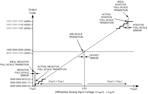 Figure 4-1 Input / Output Transfer Characteristic
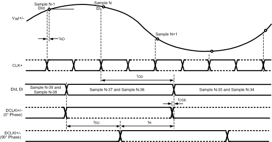
The timing for these figures is shown for the one input only (I or Q). However, both I- and Q-inputs may be used. For this case, the I-channel functions precisely the same as the Q-channel, with VinI, DCLKI, DId and DI instead of VinQ, DCLKQ, DQd and DQ. Both I- and Q-channel use the same CLK.
Figure 4-2 Clocking in 1:2 Demux Non-DES Mode
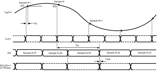
The timing for these figures is shown for the one input only (I or Q). However, both I- and Q-inputs may be used. For this case, the I-channel functions precisely the same as the Q-channel, with VinI, DCLKI, DId and DI instead of VinQ, DCLKQ, DQd and DQ. Both I- and Q-channel use the same CLK.
Figure 4-3 Clocking in Non-Demux Non-DES Mode
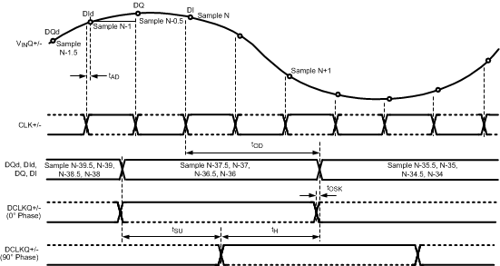
The timing for these figures is shown for the one input only (I or Q). However, both I- and Q-inputs may be used. For this case, the I-channel functions precisely the same as the Q-channel, with VinI, DCLKI, DId and DI instead of VinQ, DCLKQ, DQd and DQ. Both I- and Q-channel use the same CLK.
Figure 4-4 Clocking in 1:4 Demux DES Mode
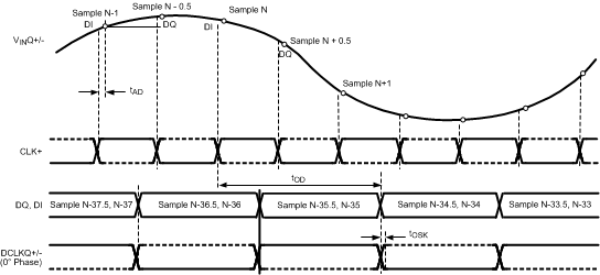
The timing for these figures is shown for the one input only (I or Q). However, both I- and Q-inputs may be used. For this case, the I-channel functions precisely the same as the Q-channel, with VinI, DCLKI, DId and DI instead of VinQ, DCLKQ, DQd and DQ. Both I- and Q-channel use the same CLK.
Figure 4-5 Clocking in Non-Demux Mode DES Mode
 Figure 4-6 Data Clock Reset Timing (Demux Mode)
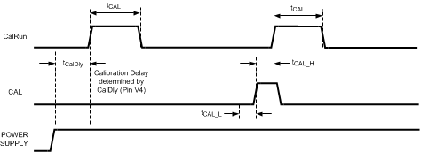 Figure 4-7 Power-on and On-Command Calibration Timing
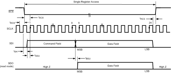 Figure 4-8 Serial Interface Timing
4.16 Typical Characteristics
VA = VDR = VTC = VE = 1.9V, fCLK = 1.8 GHz, fIN = 498 MHz, TA= 25°C, I-channel, 1:2 Demux Non-DES Mode (1:1 Demux Non-DES Mode has similar performance), unless otherwise stated. For NPR plots, notch width = 25 MHz, fc = 320 MHz.
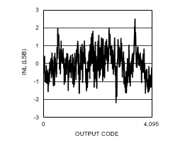 Figure 4-9 INL vs. Code (ADC12D1800)
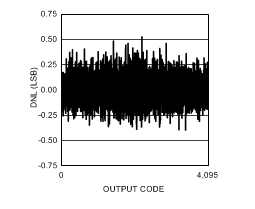 Figure 4-11 DNL vs. Code (ADC12D1800)
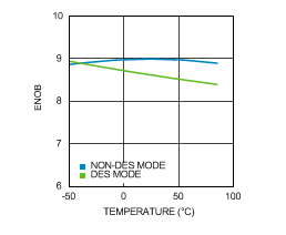 Figure 4-13 ENOB vs. Temperature (ADC12D1800)
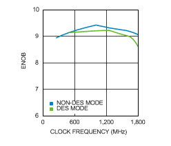 Figure 4-15 ENOB vs. Clock Frequency (ADC12D1800)
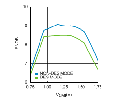 Figure 4-17 ENOB vs. VCMI (ADC12D1800)
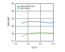 Figure 4-19 SNR vs. Supply Voltage (ADC12D1800)
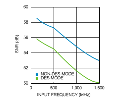 Figure 4-21 SNR vs. Input Frequency (ADC12D1800)
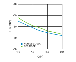 Figure 4-23 THD vs. Supply Voltage (ADC12D1800)
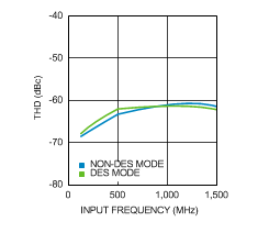 Figure 4-25 THD vs. Input Frequency (ADC12D1800)
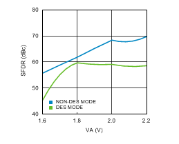 Figure 4-27 SFDR vs. Supply Voltage (ADC12D1800)
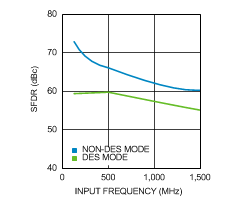 Figure 4-29 SFDR vs. Input Frequency (ADC12D1800)
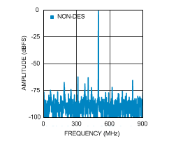 Figure 4-31 Spectral Response at FIN = 498 MHz (ADC12D1800)
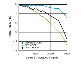 Figure 4-33 Full Power Bandwidth (ADC12D1800)
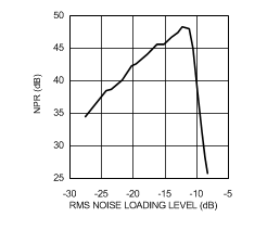 Figure 4-35 NPR vs. RMS Noise Loading Level (ADC12D1800)
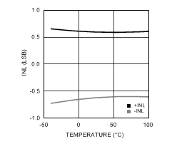 Figure 4-10 INL vs. Temperature (ADC12D1800)
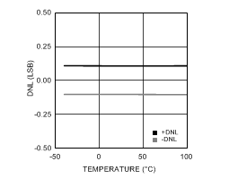 Figure 4-12 DNL vs. Temperature (ADC12D1800)
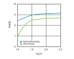 Figure 4-14 ENOB vs. Supply Voltage (ADC12D1800)
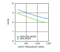 Figure 4-16 ENOB vs. Input Frequency (ADC12D1800)
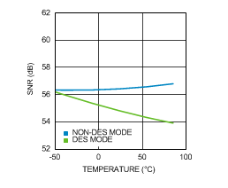 Figure 4-18 SNR vs. Temperature (ADC12D1800)
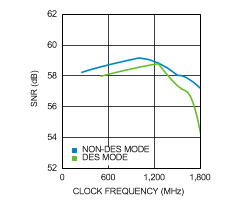 Figure 4-20 SNR vs. Clock Frequency (ADC12D1800)
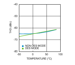 Figure 4-22 THD vs. Temperature (ADC12D1800)
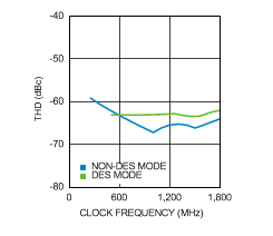 Figure 4-24 THD vs. Clock Frequency (ADC12D1800)
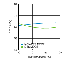 Figure 4-26 SFDR vs. Temperature (ADC12D1800)
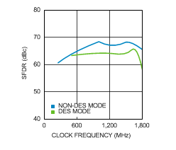 Figure 4-28 SFDR vs. Clock Frequency (ADC12D1800)
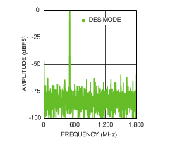 Figure 4-30 Spectral Response at FIN = 498 MHz (ADC12D1800)
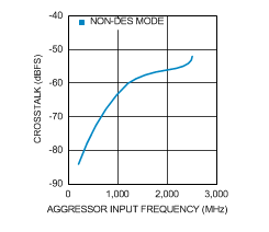 Figure 4-32 Crosstalk vs. Source Frequency (ADC12D1800)
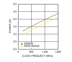 Figure 4-34 Power Consumption vs. Clock Frequency (ADC12D1800)