SNAS466G February 2009 – December 2016 ADC10D1000QML-SP
PRODUCTION DATA.
- 1 Features
- 2 Applications
- 3 Description
- 4 Revision History
- 5 Pin Configuration and Functions
-
6 Specifications
- 6.1 Absolute Maximum Ratings
- 6.2 ESD Ratings
- 6.3 Recommended Operating Conditions
- 6.4 Thermal Information
- 6.5 Converter Electrical Characteristics: Static Converter Characteristics
- 6.6 Converter Electrical Characteristics: Dynamic Converter Characteristics
- 6.7 Converter Electrical Characteristics: Analog Input/Output and Reference Characteristics
- 6.8 Converter Electrical Characteristics: Channel-to-Channel Characteristics
- 6.9 Converter Electrical Characteristics: LVDS CLK Input Characteristics
- 6.10 Electrical Characteristics: AutoSync Feature
- 6.11 Converter Electrical Characteristics: Digital Control and Output Pin Characteristics
- 6.12 Converter Electrical Characteristics: Power Supply Characteristics (1:2 Demux Mode)
- 6.13 Converter Electrical Characteristics: AC Electrical Characteristics
- 6.14 Timing Requirements: Serial Port Interface
- 6.15 Timing Requirements: Calibration
- 6.16 Quality Conformance Inspection
- 6.17 Timing Diagrams
- 6.18 Typical Characteristics
-
7 Detailed Description
- 7.1 Overview
- 7.2 Functional Block Diagram
- 7.3 Feature Description
- 7.4
Device Functional Modes
- 7.4.1
Control Modes
- 7.4.1.1
Non-Extended Control Mode
- 7.4.1.1.1 Non-Demultiplexed Mode Pin (NDM)
- 7.4.1.1.2 Dual Data-Rate Phase Pin (DDRPh)
- 7.4.1.1.3 Calibration Pin (CAL)
- 7.4.1.1.4 Power-Down I-Channel Pin (PDI)
- 7.4.1.1.5 Power-Down Q-Channel Pin (PDQ)
- 7.4.1.1.6 Test Pattern Mode Pin (TPM)
- 7.4.1.1.7 Full-Scale Input Range Pin (FSR)
- 7.4.1.1.8 AC-DC-Coupled Mode Pin (VCMO)
- 7.4.1.1.9 LVDS Output Common-Mode Pin (VBG)
- 7.4.1.1
Non-Extended Control Mode
- 7.4.2 Extended Control Mode
- 7.4.1
Control Modes
- 7.5 Programming
- 7.6 Register Maps
- 8 Application and Implementation
- 9 Power Supply Recommendations
- 10Layout
- 11Device and Documentation Support
- 12Mechanical, Packaging, and Orderable Information
10 Layout
10.1 Layout Guidelines
10.1.1 Board Mounting Recommendation
Proper thermal profile is required to establish re-flow under the package and ensure all joints meet profile specifications, See Table 31.
Table 31. Solder Profile Specification
| RANGE UP | PEAK TEMPERATURE (TPK) | MAXIMUM PEAK TEMPERATURE | RAMP DOWN |
|---|---|---|---|
| ≤ 4°C/sec | 210°C ≤ tPK ≤ 215°C | ≤ 220°C | ≤ 5°C/sec |
The 220°C peak temperature is driven by the requirement to limit the dissolution of lead from the high-melt column to the eutectic solder. Too much lead increases the effective melting point of the board-side joint and makes it much more difficult to remove the part if module rework is required.
Cool-down rates and methods affect CCGA assemble yield and reliability. Picking up boards or opening the oven while solder joints are in molten state can disturb the solder joint. Do not pick up boards until the solder joints have fully solidified. Board warping may potentially cause the CCGA to lift off of pads during cooling and this condition can also cause column cracking when severe. This warping is a result of a high differential cooling rate between the top and bottom of the board. Both conditions can be prevented by using even top and bottom cooling.
10.2 Layout Example
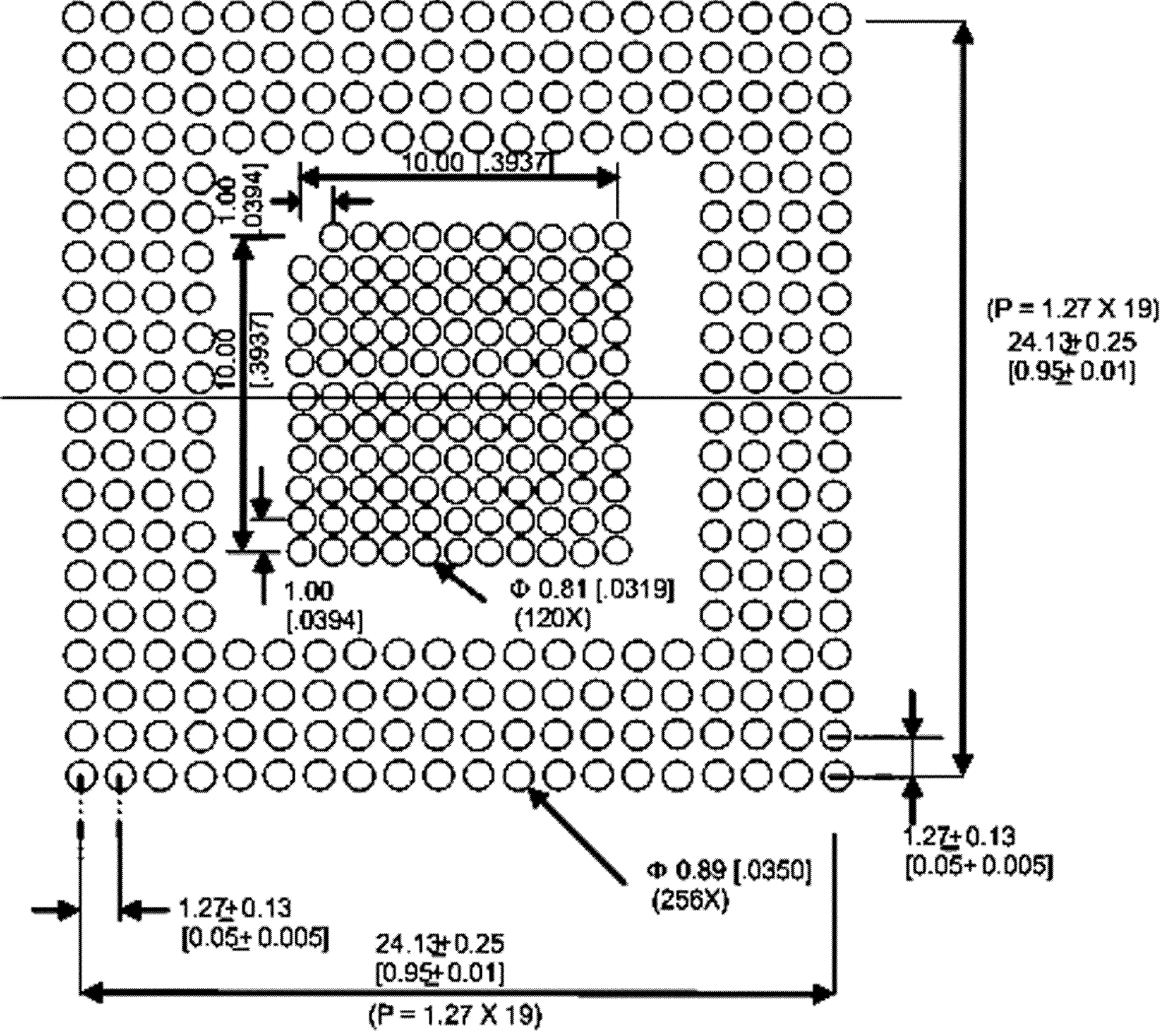
 Figure 50. Landing Pattern Recommendation
10.3 Thermal Management
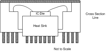
The ceramic column grid array (CCGA) package is a modified ceramic land grid array with an added heat sink. The signal columns on the outer edge are 1.27-mm pitch, while the columns in the center attached to the heat sink are 1 mm. The smaller pitch for the center columns is to improve the thermal resistance. The center columns of the package are attached to the back of the die through a heat sink. Connecting these columns to the PCB ground planes with a low thermal resistance path is the best way to remove heat from the ADC. These pins must also be connected to the ground planes through low impedance path for electrical purposes.
 Figure 51. CCGA Conceptual Drawing
10.4 Temperature Sensor Diode
The ADC10D1000 has an on-die temperature diode connected to pins Tdiode+, Tdiode– which may be used to monitor the die temperature. Texas Instruments also provides a family of temperature sensors for this application which monitor different numbers of external devices, See Table 32.
Table 32. Temperature Sensor Recommendation
| NUMBER OF EXTERNAL DEVICES MONITORED | RECOMMENDED TEMPERATURE SENSOR |
|---|---|
| 1 | LM95235 |
| 2 | LM95213 |
| 4 | LM95214 |
The LM95235/13/14 is an 11-bit digital temperature sensor with a 2-wire system management bus (SMBus) interface that can monitor the temperature of one/two/four remote diodes as well as its own temperature. The LM95235/13/14 can be used to accurately monitor the temperature of up to one/two/four external devices such as the ADC10D1000, a FPGA, other system components, and the ambient temperature.
The LM95235/13/14 reports temperature in two different formats for 127.875°C range and 0°/255°C range. The LM95235/13/14 has a sigma-delta ADC core which provides the first level of noise immunity. For improved performance in a noise environment, the LM9535/13/14 includes programmable digital filters for remote diode temperature readings. When the digital filters are invoked, the resolution for the remote diode readings increases to 0.03125°C. For maximum flexibility and best accuracy, the LM95235/13/14 includes offset registers that allow calibration of other diode types.
Diode fault detection circuitry in the LM95235/13/14 can detect the absence or fault state of a remote diode: whether the D+ pin is detected as shorted to GND, D-, VDD or D+ is floating.
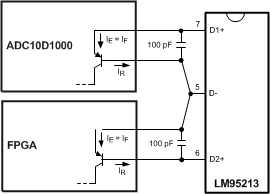
In the following typical application, the LM95213 is used to monitor the temperature of an ADC10D1000 as well as an FPGA. See Figure 52.
 Figure 52. Typical Temperature Sensor Application
10.5 Radiation Environments
Give careful consideration to environmental conditions when using a product in a radiation environment.
10.5.1 Total Ionizing Dose
Radiation hardness assured (RHA) products are those part numbers with a total ionizing dose (TID) level specified in on the front page. Testing and qualification of these products is done on a wafer level according to MIL-STD-883, Test Method 1019. Wafer-level TID data is available with lot shipments.
10.5.2 Single Event Latch-Up and Functional Interrupt
One time single event latch-up (SEL) and single event functional interrupt (SEFI) testing was preformed according to EIA/JEDEC Standard, EIA/JEDEC57. The linear energy transfer threshold (LETth) shown in Features is the maximum LET tested. A test report is available upon request.
10.5.3 Single Event Upset
A report on single event upset (SEU) is available at www.ti.com/radiation.