SN55LVTA4-SEP
- VID V62/25605-01XE
- Total ionizing dose characterized at 30krad (Si)
- Total ionizing dose radiation lot acceptance testing (TID RLAT) for every wafer lot to 30krad (Si)
- Single-event effects (SEE) characterized:
- Single event latch-up (SEL) immune to linear energy transfer (LET) = 50MeV-cm2 /mg
- Single event transient (SET) characterized to 50MeV-cm2/mg.
- Meet or exceed the requirements of ANSI TIA/EIA-644 standard
- Low-voltage differential signaling with typical output voltage of 350mV and 100Ω load
- Typical output voltage rise and fall times of 500ps (400Mbps)
- Typical propagation delay times of 1.7ns
- Operate from a single 3.3V supply
- Power dissipation 25mW typical per driver at 200MHz
- Driver at high impedance when disabled or with VCC = 0
- Bus-terminal ESD protection exceeds 8kV
- Low-voltage TTL (LVTTL) logic input levels
- Cold sparing for space and high reliability applications requiring redundancy
- Space enhanced plastic (SEP)
- Controlled baseline
- Gold wire, NiPdAu lead finish
- One assembly and test site, one fabrication site
- Extended product life cycle
- Military (–55°C to 125°C) temperature range
- Product traceability
- Meets NASA ASTM E595 outgassing specification
The SN55LVTA4-SEP is a differential line driver that implements the electrical characteristics of low-voltage differential signaling (LVDS) with a 3.3V supply. This driver delivers a minimum differential output voltage magnitude of 247mV into a 100Ω load when enabled.
The intended application of this device and signaling technique is both point-to-point and multi-drop (one driver and multiple receivers) data transmission over controlled impedance media of approximately 100Ω. The transmission media can be printed-circuit board traces, backplanes, or cables. The ultimate rate and distance of data transfer is dependent upon the attenuation characteristics of the media and the noise coupling to the environment.
The SN55LVTA4-SEP is characterized for operation from –55°C to 125°C.
您可能會感興趣的類似產品
功能相似於所比較的產品。
技術文件
| 重要文件 | 類型 | 標題 | 格式選項 | 下載最新的英文版本 | 日期 | |
|---|---|---|---|---|---|---|
| * | 資料表 | SN55LVTA4-SEP Radiation Tolerant Quad Channel High-Speed Differential Line Driver datasheet (Rev. A) | PDF | HTML | 2025/6/30 | ||
| * | 輻射及可靠性報告 | SN55LVTA4-SEP Single-Event Effects (SEE) Radiation Report | PDF | HTML | 2025/6/23 | ||
| * | 輻射及可靠性報告 | SN55LVTA4-SEP Total Ionizing Dose (TID) Report | PDF | HTML | 2025/6/23 | ||
| * | 輻射及可靠性報告 | SN55LVTA4-SEP Production Flow and Reliability Report | PDF | HTML | 2025/6/3 | ||
| * | VID | SN55LVTA4-SEP VID SN55LVTA4-SEP VID V62/25605 | 2026/5/5 | |||
| Application brief | LVDS Designs for SpaceWire | PDF | HTML | 2026/10/14 | |||
| 選擇指南 | TI Space Products (Rev. L) | 2026/3/27 |
設計與開發
如需其他條款或必要資源,請按一下下方的任何標題以檢視詳細頁面 (如有)。
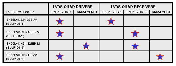
SN65LVDS31-33EVM — 適用 SN65LVDS31 和 SN65LVDS33 的評估模組
TI offers a series of low-voltage differential signaling (LVDS) evaluation modules (EVMs) designed for analysis of the electrical characteristics of LVDS drivers and receivers. Four unique EVMs are available to evaluate the different classes of LVDS devices offered by TI.
As seen in the Combination (...)
| 封裝 | 針腳 | CAD 符號、佔位空間與 3D 模型 |
|---|---|---|
| SOIC (D) | 16 | Ultra Librarian |
訂購與品質
建議產品可能具有與此 TI 產品相關的參數、評估模組或參考設計。