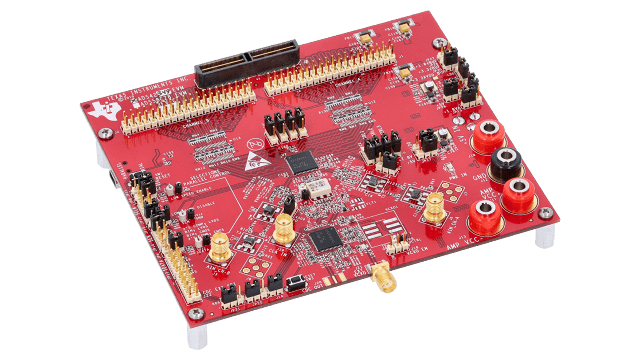
ADS42B49EVM 的特性
- Transformer coupled analog input path
- Amplifier path based on the THS4509
- Configurable CMOS or DDR LVDS parallel output modes
- Transformer coupled clock input path
- CDCE72010 Jitter Clock Synchronizer and Jitter Cleaner clocking circuit
- DDR LVDS output and capture ability via TSW1200 capture card
- USB controlled for SPI access
ADS42B49EVM 的说明
The ADS42B49EVM is a circuit board that allows designers to evaluate the performance of Texas Instruments‘ ADS42B49 device, an extremely low power dual channel 14-bit 250 MSPS analog to digital converter. The ADC features a configurable parallel DDR LVDS or CMOS outputs. The EVM provides a flexible environment to test the ADS42B49 under a variety of clock, input and supply conditions.
The ADS42B49EVM also includes Texas Instrument’s new 10 Output Low Jitter Clock Synchronizer and Jitter Cleaner device, the CDCE72010, which can be used to drive the clocking input to the ADS42B49. Open sockets are provided for an external VCXO and crystal band pass filter allowing for rapid evaluation of a combined high performance ADC and clocking circuit equivalent to a final system level solution. Alternatively an external clock source can be provided to the EVM and either routed through the CDCE72010 or passed directly to the ADS42B49 clock input.
The ADS42B49EVM is directly compatible to the TSW1400EVM and TSW1405EVM, TI's high speed LVDS output ADC data capture cards. It is also compatible with Altera and Xilinx FPGA EVMs which have FMC or HSMC connectors, via the appropriate interposer card.