Buffer Op Amp to Analog-to-Digital Converter Design: Single-Ended Input, Single Supply, Transformer Coupled
Problem:
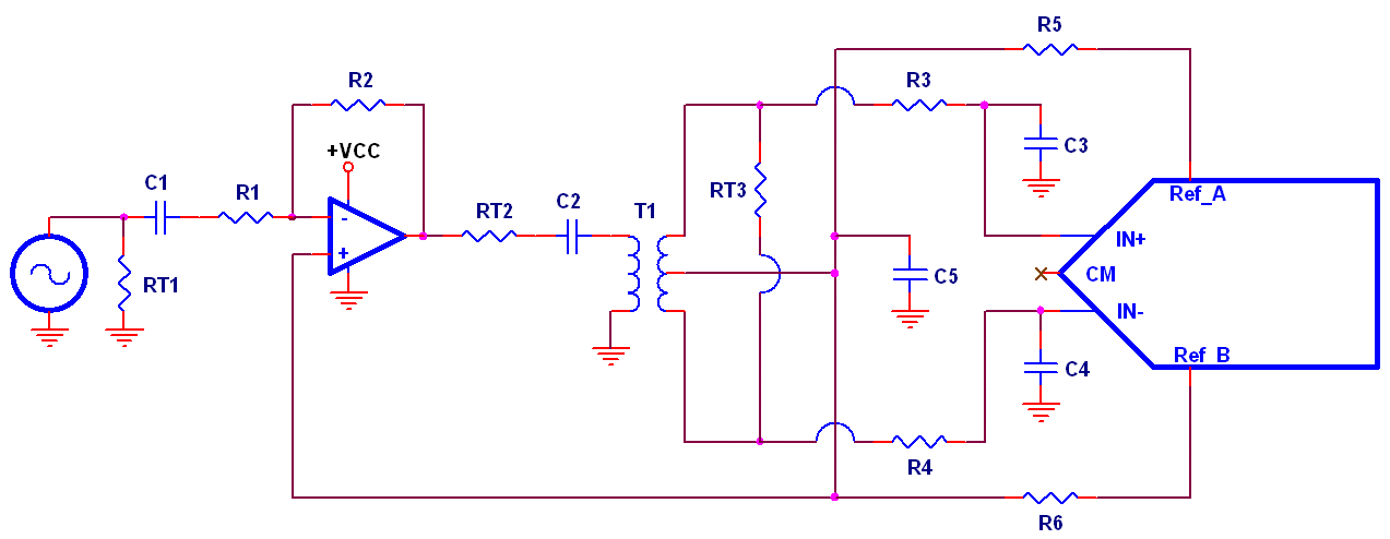
How do I buffer the input of an Analog to Digital Converter (ADC) when I have a single-ended input, single power supply and transformer coupling?
Solution:

Double click on schematic to enlarge.
The gain for the inverting stage is determined by R2 and R1. RT2 Isolates the op amp output from the reactive load formed by C1 and the primary of T1, and also operates to terminate the input. The
common mode input for the secondary of T1 and the virtual ground for the buffer op amp stage is generated by Resistors R5 and R6, and bypassed by C5. R5 and R6 should be matched. R3, R4, C2, and C3
are ADC compensation components. RT1 terminates the input source, RT2 terminates the transformer primary, and RT3 terminates the transformer secondary (calculated by the turn ratio of the
transformer).