Buffer Op Amp to Analog-to-Digital Converter Design: Single-Ended Input, Dual Supply, Transformer Coupled
Problem:
How do I buffer the input of an Analog to Digital Converter (ADC) when I have a single-ended input, dual power supply and transformer coupling?
Solution:
Double click on schematic to enlarge.
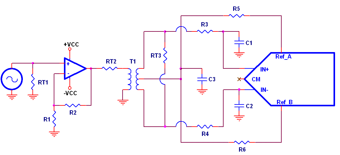
Resistors R1 and R2 set the non-inverting gain of the op amp to the desired level. Resistor RT2 isolates the output of the op amp from the inductive load created by the primary of T1. It also acts
as a matching resistor for termination resistor RT3, which terminates the secondary of transformer. Resistors R3 and R4, and capacitors C1 and C2 are ADC compensation components. Resistors R5 and
R6, which should be matched, are used to derive a common mode reference. The reference derived from Resistors R5 and R6 is connected to the center tap of the secondary of T1, which sets the common
mode point for the signals connected to IN+ and IN-. Capacitor C3 bypasses the derived common mode reference.