Buffer Op Amp to Analog-to-Digital Converter Design: DC Coupled Single-Ended Input, Single Supply, Single-Ended Op Amps, Single Input to ADC
Problem:
How do I buffer the input of an Analog to Digital Converter (ADC) when I have an DC coupled single-ended input, single power supply, single-ended op amps, and single input to ADC?
Solution:
Double click on schematic to enlarge.
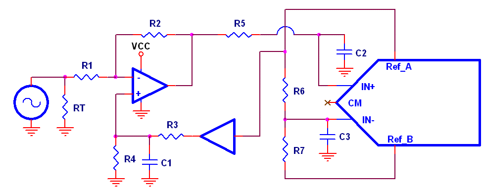
R1 and R2 are selected to provide inverting gain. The non-inverting input is used to input a dc reference derived from Ref_A, which is divided to the correct level by resistors R3 and R4. The op
amp provides non-inverting dc gain on this divided reference, boosting it to the common mode voltage level of the ADC. R6 and R7 generate the same common mode voltage and supply it to the ADC on its
IN- input. C1 and C3 are decoupling capacitors. R5 and C2 are compensation components specified by the ADC data sheet. This circuit is not as desirable as some others, because it will be difficult
to keep the reference provided to the op amp at the same level as the reference presented to the ADC.
The Ref_A output of the ADC probably does not have enough drive capability to drive the resistive voltage divider, and must be buffered. This buffer is shown as a generic amplifier - it can be as
simple as a non-inverting op amp buffer or more sophisticated if low drift is needed.