Buffer Op Amp to Analog-to-Digital Converter Design: AC Coupled Single-Ended Input, Single Supply, Single-Ended Op Amps, Single Input to ADC
Problem:
How do I buffer the input of an Analog to Digital Converter (ADC) when I have an AC coupled single-ended input, single power supply, single-ended op amps, and single input to ADC?
Solution:
Double click on schematic to enlarge.
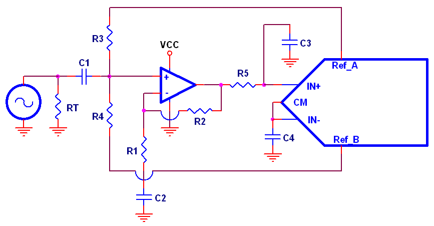
The ADC IN- input is connected to the common mode output of the ADC, and decoupled with C4. This sets the input range of the ADC as the common mode voltage to +Ref_A. The input source
is coupled through C1 to the non-inverting input of the op amp. Non-inverting stage gain is set by R2 and R1. The local virtual ground is created from Ref_A and Ref_B though resistors R3 and R4,
which should be equal in value. Capacitor C2 isolates the virtual ground potential. R5 and C3 are ADC compensation components. This circuit may have a dc error due to the fact that the common
mode input to IN+ will be slightly different than the dc potential created by R3 and R4.