Buffer Op Amp to Analog-to-Digital Converter Design: AC Coupled Single-Ended Input, Single Supply, Single-Ended Op Amps, Differential Input to ADC
Problem:
How do I buffer the input of an Analog to Digital Converter (ADC) when I have an AC coupled single-ended input, single power supply, single-ended op amps, and differential input to ADC?
Solution:
Double click on schematic to enlarge.
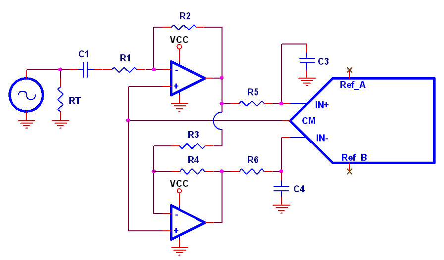
In this implementation, both stages are inverting stages. Gain is accomplished in the first stage with R1 as the input resistor and R2 as the gain resistor. R3 and R4 are equal, creating a
unity-inverting gain inverting stage. The common mode output of the ADC provides the virtual ground for both stages. The advantage of this approach is that C2, the second dc blocking capacitor, is
eliminated. The disadvantage, of course, is that the bottom signal is delayed by the additional delay of the bottom stage with respect to the top. Therefore, the input signal will arrive at IN+
before it will at IN-.