Buffer Op Amp to Analog-to-Digital Converter Design: AC Coupled Single-Ended Input, Single Supply, Single-Ended Op Amps, Differential Input to ADC
Problem:
How do I buffer the input of an Analog to Digital Converter (ADC) when I have an AC coupled single-ended input, single power supply, single-ended op amps, and differential input to ADC?
Solution:
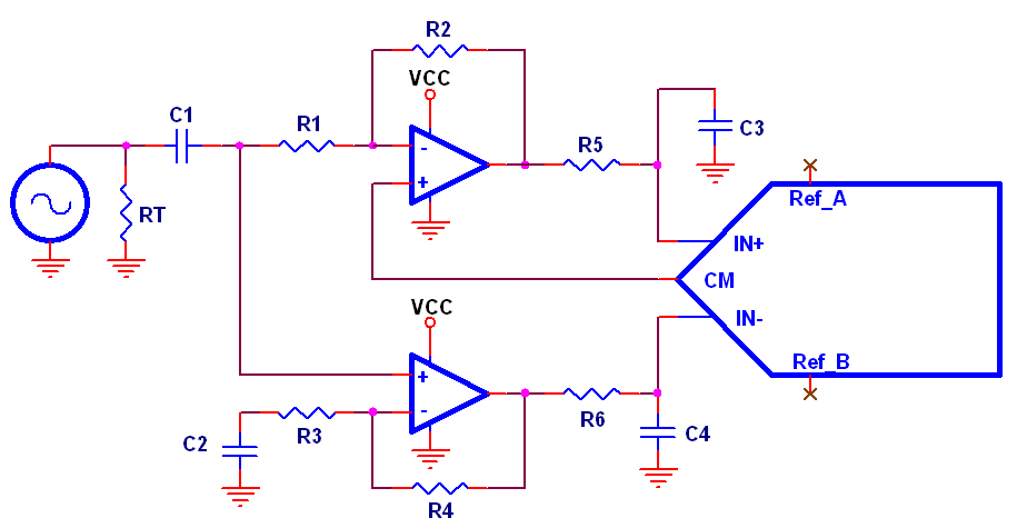
Double click on schematic to enlarge.
This implementation takes advantage of the characteristics of inverting and non-inverting op amp stages. The common mode voltage from the ADC is coupled to the inverting op amp
stage on the top as its virtual ground. This dc voltage is superimposed on the ac coupled signal its virtual ground. There is no dc return, so there is no dc gain. The virtual ground potential
appears at the op amp output, the inverting input, and because no dc current flows through blocking capacitor C1 - the junction of R1 and C1. This potential is also connected to the non-inverting
input of the bottom op amp stage, and appears at its output and inverting input as well. Because C2 also blocks dc current, the dc voltage is prevented from being amplified by 2 in the bottom stage,
which looks like a unity gain buffer to dc. R5, R6, C3, and C4 are ADC compensation components.
The chief disadvantage of this approach is that it is hard to come up with resistor values that will match the inverting and non-inverting stages. If the circuit is to be unity gain, R1 and R2
should be the same value, and R2 and C3 can be omitted.