Buffer Op Amp to Analog-to-Digital Converter Design: DC Coupled Single-Ended Input, Single Supply, Differential Op Amps, Differential Input to ADC
Problem:
How do I buffer the input of an Analog to Digital Converter (ADC) when I have an DC coupled single-ended input, single power supply, differential op amps, and differential input to ADC?
Solution:
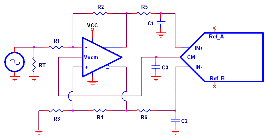
Double click on schematic to enlarge.
This is a challenge. The termination resistor RT, in parallel with the source impedance, forms a portion of the gain resistor R1. Changing the gain resistor, of course, also changes the gain of the
stage, and unbalances the top and bottom feedback pathways. Re-balancing the feedback paths changes the gain, etc. The design process is iterative, and goal seeking. Texas Instruments has an engineering design utility to handle this case.