Buffer Op Amp to Analog-to-Digital Converter Design: AC Coupled Single-Ended Input, Dual Supply, Differential Op Amps, Differential Input to ADC
Problem:
How do I buffer the input of an Analog to Digital Converter (ADC) when I have an AC coupled single-ended input, dual power supply, differential op amps, and differential input to ADC?
Solution:
Double click on schematic to enlarge.
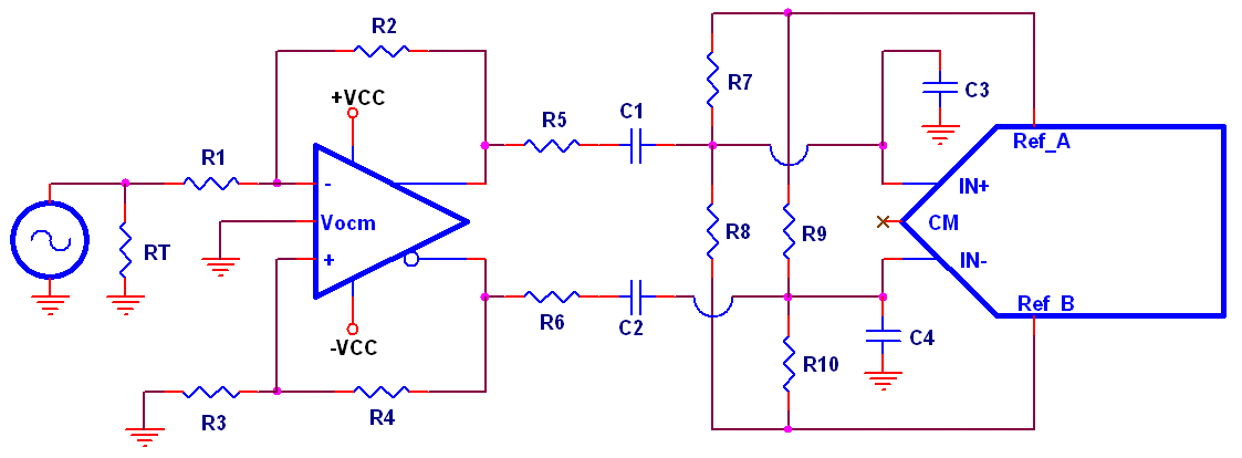
If a termination resistor is used, this presents a challenge for the designer. The termination resistor RT, in parallel with the source impedance, forms a portion of the gain resistor R1. Changing
the gain resistor, of course, also changes the gain of the stage, and unbalances the top and bottom feedback pathways. Re-balancing the feedback paths changes the gain, etc. The design process is
iterative, and goal seeking. Texas Instruments has an engineering design utility to handle this case.
Resistors R1 through R4 set the gain of the stage. Capacitors C1 and C2 are ac coupling capacitors. Resistors R7 through R10 sets the common mode voltage of the two inputs. R5, R6, C3, and C4 are
ADC compensation components.