Buffer Op Amp to Analog-to-Digital Converter Design: DC Coupled Differential Input, Single Supply, Differential Op Amps, Differential Input to ADC
Problem:
How do I buffer the input of an Analog to Digital Converter (ADC) when I have an DC coupled differential input, single power supply, differential op amps, and differential input to ADC?
Solution:

Double click on schematic to enlarge.
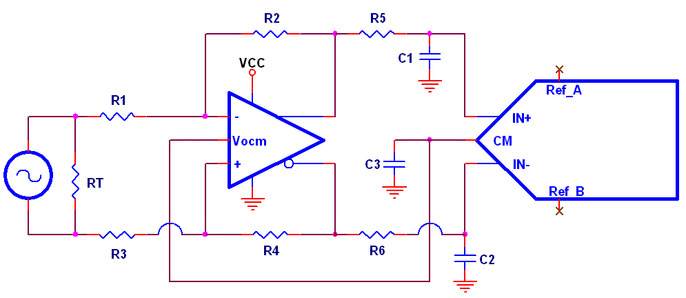
A differential voltage source is terminated with a termination resistor RT. Resistors R1 through R4 set the gain of the fully differential op amp. R5, R6, C1, and C2 are compensation components
specified on the ADC data sheet. The common mode voltage for this circuit comes from the source, and is bypassed by capacitor C3. The common mode voltage appearing on the source will be rejected,
and the common mode voltage of the ADC is the common mode point of the circuit.