Buffer Op Amp to Analog-to-Digital Converter Design: AC Coupled Differential Input, Single Supply, Differential Op Amps, Differential Input to ADC
Problem:
How do I buffer the input of an Analog to Digital Converter (ADC) when I have an AC coupled differential input, single power supply, differential op amps, and differential input to ADC?
Solution:
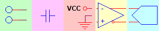

Double click on schematic to enlarge.
A differential voltage source is terminated with a termination resistor RT. Capacitors C1 and C2 are ac coupling capacitors. They should be equal in value to balance both feedback pathways of the
op amp. The designer should remember that the capacitors will appear in series and be effectively reduced to half their value. Resistors R1 through R4 set the gain of the fully differential op amp.
R5, R6, C5, and C4 are compensation components specified on the ADC data sheet. Capacitor C3 decouples the common mode output of the ADC.