SLVSAC3D May 2011 – December 2014 TPS62730 , TPS62732 , TPS62733
PRODUCTION DATA.
- 1 Features
- 2 Applications
- 3 Description
- 4 Revision History
- 5 Description (Continued)
- 6 Device Comparison Table
- 7 Pin Configuration and Functions
- 8 Specifications
- 9 Detailed Description
- 10Application and Implementation
- 11Power Supply Recommendations
- 12Layout
- 13Device and Documentation Support
- 14Mechanical, Packaging, and Orderable Information
Package Options
Mechanical Data (Package|Pins)
- DRY|6
Thermal pad, mechanical data (Package|Pins)
- DRY|6
Orderable Information
1 Features
- Input Voltage Range VIN From 1.9 V to 3.9 V
- Typ. 30-nA Ultra Low-Power Bypass Mode
- Typ. 25-μA DC-DC Quiescent Current
- Internal Feedback Divider Disconnect
- Typical 2.1-Ω Bypass Switch Between VIN and VOUT
- Automatic Transition from DC-DC to Bypass Mode
- Up to 3-MHz Switch Frequency
- Up to 95% DC-DC Efficiency
- Open-Drain Status Output STAT
- Output Peak Current up to 100 mA
- Fixed Output Voltages 1.9 V, 2.05 V, 2.1 V, 2.3 V
- Small External Output Filter Components 2.2 μH and 2.2 μF
- Optimized For Low Output Ripple Voltage
- Small 1 × 1.5 × 0.6-mm3 USON Package
- 12-mm2 Minimum Solution Size
2 Applications
- CC2540 Bluetooth™ Low-Energy
System-On-Chip Solution - Low-Power Wireless Applications
- RF4CE, Metering
3 Description
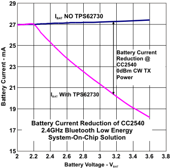
The TPS62730 is a high frequency synchronous step-down DC-DC converter optimized for ultra low-power wireless applications. The device is optimized to supply TI's Low-Power Wireless sub 1-GHz and 2.4-GHz RF transceivers and System-On-Chip (SoC) solutions. The TPS62730 reduces the current consumption drawn from the battery during TX and RX mode by a high efficient step-down voltage conversion. The device provides an output current of up to 100 mA and allows the use of tiny and low-cost chip inductors and capacitors. With an input voltage range of 1.9 V to 3.9 V, the device supports Li-primary battery chemistries such as Li-SOCl2, Li-SO2, Li-MnO2, and also two cell alkaline batteries.
The TPS62730 features an Ultra Low-Power bypass mode with typical 30-nA current consumption to support sleep and low power modes of TI's CC2540 Bluetooth Low Energy and CC430 SoC solutions. In this bypass mode, the output capacitor of the DC-DC converter is connected through an integrated typical 2.1-Ω bypass switch to the battery.
Device Information(1)
| PART NUMBER | PACKAGE | BODY SIZE (NOM) |
|---|---|---|
| TPS62730 | USON (6) | 1.45 mm x 1.00 mm |
| TPS62732 | ||
| TPS62733 |
- For all available packages, see the orderable addendum at the end of the datasheet.
Typical Application
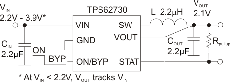
Battery Current Reduction Using TPS62730