SPRS737C August 2011 – April 2014 TMS320C5532 , TMS320C5533 , TMS320C5534 , TMS320C5535
PRODUCTION DATA.
- 1Device Overview
- 2Revision History
- 3Device Comparison
-
4Terminal Configuration and Functions
- 4.1 Pin Diagram
- 4.2
Signal Descriptions
- 4.2.1 Oscillator and PLL
- 4.2.2 Real-Time Clock (RTC)
- 4.2.3 RESET, Interrupts, and JTAG
- 4.2.4 Inter-Integrated Circuit (I2C)
- 4.2.5 Inter-IC Sound (I2S)
- 4.2.6 Serial Peripheral Interface (SPI)
- 4.2.7 Universal Asynchronous Receiver/Transmitter (UART)
- 4.2.8 Universal Serial Bus (USB) 2.0
- 4.2.9 LCD Bridge
- 4.2.10 Secure Digital (SD)
- 4.2.11 Successive Approximation (SAR) Analog-to-Digital Converter (ADC)
- 4.2.12 General-Purpose Input/Output (GPIO)
- 4.2.13 Regulators and Power Management
- 4.2.14 Reserved and No Connects
- 4.2.15 Supply Voltage
- 4.2.16 Ground
- 4.3 Pin Multiplexing
-
5Specifications
- 5.1 Absolute Maximum Ratings
- 5.2 Recommended Operating Conditions
- 5.3 Electrical Characteristics
- 5.4 Handling Ratings
- 5.5 Thermal Characteristics
- 5.6 Power-On Hours
- 5.7
Timing and Switching Characteristics
- 5.7.1 Parameter Information
- 5.7.2
Power Supplies
- 5.7.2.1 Power Considerations for C5535 and C5534
- 5.7.2.2 Power Considerations for C5533
- 5.7.2.3 Power Considerations for C5532
- 5.7.2.4 Power-Supply Sequencing
- 5.7.2.5 Digital I/O Behavior When Core Power (CVDD) is Down
- 5.7.2.6 Power-Supply Design Considerations
- 5.7.2.7 Power-Supply Decoupling
- 5.7.2.8 LDO Input Decoupling
- 5.7.2.9 LDO Output Decoupling
- 5.7.3
Reset
- 5.7.3.1 Power-On Reset (POR) Circuits
- 5.7.3.2 Pin Behavior at Reset
- 5.7.3.3 Reset Electrical Data and Timing
- 5.7.3.4 Configurations at Reset
- 5.7.3.5
Configurations After Reset
- 5.7.3.5.1 External Bus Selection Register (EBSR)
- 5.7.3.5.2 LDO Control Register [7004h]
- 5.7.3.5.3 USB System Control Registers (USBSCR) [1C32h]
- 5.7.3.5.4 Peripheral Clock Gating Control Registers (PCGCR1 and PCGCR2) [1C02h and 1C03h]
- 5.7.3.5.5 Pullup and Pulldown Inhibit Registers (PDINHIBR1, 2, and 3) [1C17h, 1C18h, and 1C19h]
- 5.7.3.5.6 Output Slew Rate Control Register (OSRCR) [1C16h]
- 5.7.4
Clock Specifications
- 5.7.4.1 Recommended Clock and Control Signal Transition Behavior
- 5.7.4.2 Clock Considerations
- 5.7.4.3 PLLs
- 5.7.4.4 Input and Output Clocks Electrical Data and Timing
- 5.7.4.5 Wake-up Events, Interrupts, and XF
- 5.7.5 Direct Memory Access (DMA) Controller
- 5.7.6 General-Purpose Input/Output
- 5.7.7 General-Purpose Timers
- 5.7.8 Inter-Integrated Circuit (I2C)
- 5.7.9 Inter-IC Sound (I2S)
- 5.7.10 Liquid Crystal Display Controller (LCDC) — C5535 Only
- 5.7.11 Real-Time Clock (RTC)
- 5.7.12 SAR ADC (10-Bit) — C5535 Only
- 5.7.13 Secure Digital (SD)
- 5.7.14 Serial Port Interface (SPI)
- 5.7.15 Universal Asynchronous Receiver/Transmitter (UART)
- 5.7.16 Universal Serial Bus (USB) 2.0 Controller — Does Not Apply to C5532
- 5.7.17 Emulation and Debug
- 5.7.18 IEEE 1149.1 JTAG
-
6Detailed Description
- 6.1 CPU
- 6.2
Memory
- 6.2.1 Internal Memory
- 6.2.2 Memory Map
- 6.2.3
Register Map
- 6.2.3.1 General-Purpose Input/Output Peripheral Register Descriptions
- 6.2.3.2 I2C Peripheral Register Descriptions
- 6.2.3.3 I2S Peripheral Register Descriptions
- 6.2.3.4 LCDC Peripheral Register Descriptions
- 6.2.3.5 RTC Peripheral Register Descriptions
- 6.2.3.6 SAR ADC Peripheral Register Descriptions
- 6.2.3.7 SD Peripheral Register Descriptions
- 6.2.3.8 SPI Peripheral Register Descriptions
- 6.2.3.9 System Registers
- 6.2.3.10 Timers Peripheral Register Descriptions
- 6.2.3.11 UART Peripheral Register Descriptions
- 6.2.3.12 USB2.0 Peripheral Register Descriptions
- 6.3 Identification
- 6.4 Boot Modes
- 7Device and Documentation Support
- 8Mechanical Packaging and Orderable Information
Package Options
Refer to the PDF data sheet for device specific package drawings
Mechanical Data (Package|Pins)
- ZAY|144
Thermal pad, mechanical data (Package|Pins)
Orderable Information
1 Device Overview
1.1 Features
- CORE:
- High-Performance, Low-Power, TMS320C55x Fixed-Point Digital Signal Processor
- 20-, 10-ns Instruction Cycle Time
- 50-, 100-MHz Clock Rate
- One or Two Instructions Executed per Cycle
- Dual Multiply-and-Accumulate Units (Up to 200 Million Multiply-Accumulates per Second [MMACS])
- Two Arithmetic and Logic Units (ALUs)
- Three Internal Data and Operand Read Buses and Two Internal Data and Operand Write Buses
- Software-Compatible with C55x Devices
- Industrial Temperature Devices Available
- 320KB of Zero-Wait State On-Chip RAM, Composed of:
- 64KB of Dual-Access RAM (DARAM), 8 Blocks of 4K x 16-Bit
- 256KB of Single-Access RAM (SARAM), 32 Blocks of 4K x 16-Bit
- 128KB of Zero Wait-State On-Chip ROM
(4 Blocks of 16K x 16-Bit) - Tightly Coupled FFT Hardware Accelerator
- PERIPHERAL:
- Direct Memory Access (DMA) Controller
- Four DMA with 4 Channels Each (16 Channels Total)
- Three 32-Bit General-Purpose (GP) Timers
- One Selectable as a Watchdog or GP
- Two Embedded Multimedia Card (eMMC) or Secure Digital (SD) Interfaces
- Universal Asynchronous Receiver/Transmitter (UART)
- Serial Port Interface (SPI) with Four Chip Selects
- Master and Slave Inter-Integrated Circuit (I2C Bus)
- Four Inter-IC Sound (I2S Bus) for Data Transport
- Device USB Port with Integrated 2.0 High-Speed PHY that Supports:
- USB 2.0 Full- and High-Speed Device
- LCD Bridge with Asynchronous Interface
- 10-Bit 4-Input Successive Approximation (SAR) ADC
- IEEE-1149.1 (JTAG)
Boundary-Scan-Compatible - 32 General-Purpose I/O (GPIO) Pins
(Multiplexed with Other Device Functions)- Configure Up to 20 GPIO Pins at the Same Time
- POWER:
- Four Core Isolated Power Supply Domains: Analog, RTC, CPU and Peripherals, and USB
- Three I/O Isolated Power Supply Domains: RTC I/O, USB PHY, and DVDDIO
- Three integrated LDOs (DSP_LDO, ANA_LDO, and USB_LDO) to power the isolated domains: DSP Core, Analog, and USB Core, respectively
- 1.05-V Core (50 MHz), 1.8-, 2.5-, 2.75-, or 3.3-V I/Os
- 1.3-V Core (100 MHz), 1.8-, 2.5-, 2.75-, or 3.3-V I/Os
- CLOCK:
- Real-Time Clock (RTC) with Crystal Input, Separate Clock Domain, and Separate Power Supply
- Low-Power Software Programmable Phase-Locked Loop (PLL) Clock Generator
- BOOTLOADER:
- On-Chip ROM Bootloader (RBL) to Boot From SPI EEPROM, SPI Serial Flash or I2C EEPROM eMMC, SD, SDHC, UART, and USB
- PACKAGE:
- 144-Terminal Pb-Free Plastic BGA (Ball Grid Array) (ZHH Suffix)
1.2 Applications
- Wireless Audio Devices (for example, Headsets, Microphones, Speakerphones)
- Echo Cancellation Headphones
- Portable Medical Devices
- Voice Applications
- Industrial Controls
- Fingerprint Biometrics
- Software-defined Radio
1.3 Description
These devices are members of TI's C5000™ fixed-point Digital Signal Processor (DSP) product family and are designed for low-power applications.
The fixed-point DSP is based on the TMS320C55x DSP generation CPU processor core. The C55x DSP architecture achieves high performance and low power through increased parallelism and total focus on power savings. The CPU supports an internal bus structure that is composed of one program bus, one 32-bit data read bus and two 16-bit data read buses, two 16-bit data write buses, and additional buses dedicated to peripheral and DMA activity. These buses provide the ability to perform up to four 16-bit data reads and two 16-bit data writes in a single cycle. The device also includes four DMA controllers, each with 4 channels, providing data movement for 16-independent channel contexts without CPU intervention. Each DMA controller can perform one 32-bit data transfer per cycle, in parallel and independent of the CPU activity.
The C55x CPU provides two multiply-accumulate (MAC) units, each capable of 17-bit x 17-bit multiplication and a 32-bit add in a single cycle. A central 40-bit arithmetic and logic unit (ALU) is supported by an additional 16-bit ALU. Use of the ALUs is under instruction set control, providing the ability to optimize parallel activity and power consumption. These resources are managed in the Address Unit (AU) and Data Unit (DU) of the C55x CPU.
The C55x CPU supports a variable byte width instruction set for improved code density. The Instruction Unit (IU) performs 32-bit program fetches from internal or external memory and queues instructions for the Program Unit (PU). The PU decodes the instructions, directs tasks to the AU and DU resources, and manages the fully protected pipeline. Predictive branching capability avoids pipeline flushes on execution of conditional instructions.
The general-purpose input and output functions, along with the 10-bit SAR ADC on the TMS320C5535, provide sufficient pins for status, interrupts, and bit I/O for LCD displays, keyboards, and media interfaces. Serial media is supported through two secure digital (SD) peripherals, four Inter-IC Sound (I2S Bus) modules, one serial port interface (SPI) with up to four chip selects, one I2C multimaster and slave interface, and a universal asynchronous receiver/transmitter (UART) interface.
Additional peripherals include: a high-speed Universal Serial Bus (USB 2.0) device mode only (not available on TMS320C5532), a real-time clock (RTC), three general-purpose timers with one configurable as a watchdog timer, and an analog phase-locked loop (APLL) clock generator.
In addition, the TMS320C5535 includes a tightly coupled FFT Hardware Accelerator. The tightly coupled FFT Hardware Accelerator supports 8- to 1024-point (in power of 2) real and complex-valued FFTs.
Furthermore, the device includes the following three integrated LDOs to power different sections of the device.
ANA_LDO (all devices) provides 1.3 V to the DSP PLL (VDDA_PLL), SAR, and power-management circuits (VDDA_ANA).
DSP_LDO (TMS320C5535 and 'C5534) provides 1.3 V or 1.05 V to the DSP core (CVDD), selectable on-the-fly by software as long as operating frequency ranges are observed. For lowest power operation, the programmer can shut down the internal DSP_LDO, cutting power to the DSP core (CVDD) while an external supply provides power to the RTC (CVDDRTC and DVDDRTC). The RTC alarm interrupt or the WAKEUP pin can re-enable the internal DSP_LDO and re-apply power to the DSP core. When DSP_LDO comes out of reset, it is enabled to 1.3 V for the bootloader to operate. For the 50-MHz devices, DSP_LDO must be programmed to 1.05 V to match the core voltage, CVDD, for proper operation after reset.
USB_LDO (TMS320C5535, 'C5534, and 'C5533) provides 1.3 V to the USB core digital (USB_VDD1P3) and PHY circuits (USB_VDDA1P3).
These devices are supported by the industry’s award-winning eXpressDSP™, Code Composer Studio™ Integrated Development Environment (IDE), DSP/BIOS™, Texas Instruments’ algorithm standard, and the industry’s largest third-party network. Code Composer Studio IDE features code generation tools including a C Compiler and Linker, RTDX™, XDS100, XDS510™, XDS560™ emulation device drivers, and evaluation modules. The devices are also supported by the C55x DSP library which features more than 50 foundational software kernels (FIR filters, IIR filters, FFTs, and various math functions) as well as chip support libraries.
Table 1-1 Device Information
| PART NUMBER | PACKAGE | BODY SIZE |
|---|---|---|
| TMS320C5535AZHH10 | BGA MICROSTAR (144) | 12.0 mm x 12.0 mm |
| TMS320C5535AZHHA10 | BGA MICROSTAR (144) | 12.0 mm x 12.0 mm |
| TMS320C5534AZHH10 | BGA MICROSTAR (144) | 12.0 mm x 12.0 mm |
| TMS320C5534AZHHA10 | BGA MICROSTAR (144) | 12.0 mm x 12.0 mm |
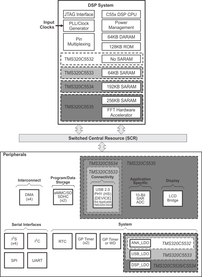
1.4 Functional Block Diagram
Figure 1-1 shows the functional block diagram of the devices.